


Abstract
Samples of inverted photonic-crystal films, containing planar and rolled-up (in the form of scrolls) CdSe nanocrystals, are studied. The transmission spectra of these structures are recorded. These spectra (along with the change in colour) confirm the incorporation of nanocrystals into the films. The photoluminescence decay dynamics is investigated. It is shown that the photonic-crystal matrix affects significantly the luminescence kinetics of nanostructures. The differences in the decay curves measured for nanocrystals in a photonic-crystal matrix and for their ensemble on a glass substrate are explained by the influence of the photonic-crystal stop band and the orientational effect of crystalline matrix, which orients anisotropic nanocrystals and prevents them from aggregation. The results obtained may be important for potential applications in optoelectronic devices.
Export citation and abstract BibTeX RIS
1. Introduction
Many properties of nanocrystals are determined by not only their sizes but also their shape. Therefore, a purposeful control of nanoparticle morphology makes it possible to design nanostructures with novel properties. Modern nanotechnologies allow for fabrication of nanoparticles of most various shapes: nanorods, nanowires, nanotubes, nanoribbons, nanospheres, nanoshells, and many others. In particular, colloidal synthesis techniques have been used to develop a new class of semiconductor quasi-two-dimensional nanocrystals based on cadmium chalcogenides: ultrathin plates with a thickness of several atomic monolayers and a well-controlled number of these layers. The absence of spread of plate thicknesses leads to elimination of dispersion of individual parameters of exciton absorption and photoluminescence in ensembles of such nanoparticles and, as a consequence, to narrowing of the corresponding spectral lines, which is very attractive for many potential applications. Other causes of the unique optical and spectral properties of these nanoplates are their spatial confinement and strong anisotropy, which are due to their very small thickness. This leads, in particular, to a giant growth of the oscillator strength of electron transitions, as well as to a high radiative recombination rate and occurrence of narrow luminescence bands (see, e.g., [1]).
In recent years technologies making it possible to form structures rolled up in the form of tubes (nanoscrolls) on the basis of the aforementioned planar semiconductor nanoplates have been developed. Since this approach opens new possibilities in the field of optical nanotechnologies, researchers show an increasing interest in the optical and luminescence properties of the nanoscale objects of new type: two-dimensional plates and three-dimensional scrolls. The quantum confinement, which leads to narrow exciton spectra of both plates and scrolls, depends on the orientation of elementary excitations relative to the object geometry, which opens up additional possibilities for using these materials in controlled optoelectronic devices. The degree of controllability of the synthesis of nanoparticles in the form of plates and scrolls constantly increases [2 – 4], and these particles have actively been used in various devices [5 – 8]. At the same time, the study of these objects meets a number of problems. The reason is as follows: when analysing an ensemble of arbitrarily located and randomly oriented nanoparticles in a volume under consideration, one cannot determine their 'true' decay kinetics and other luminescence characteristics because of the effective interaction between particles and averaging of signals from many particles. In particular, the luminescence decay kinetics is generally significantly forced during the first few nanoseconds after optical excitation due to the resonance migration of absorbed energy to neighbouring particles [9]; i.e., in essence, fast decay occurs because of the concentration quenching. The slow components are enhanced and extended, because quenching in such objects often does not completely convert excitation into heat but leads to radiative de-excitation with a delay and slightly enlarged Stokes shift; specifically this de-excitation stops resonance migration. The averaging of signal from many particles complicates the pattern even more and makes it of little use for detailed analysis. The random orientation of particles with pronounced anisotropic properties reduces the value of analysis.
The introduction of luminescent components into photonic crystals has been performed by many researchers (see, for example, review [10]). However, the introduction of nanoscrolls into photonic crystals opens up new possibilities. Indeed, one might expect that, with correctly matched sizes of crystal cells and nanoscrolls, the latter will be oriented after being incorporated into a crystal. The orientation of nanoscrolls via their introduction into photonic crystals is not the only advantage of the aforementioned method, because particles barely interact with each other in this case. As a result, one can obtain data on the properties of isolated nanoscrolls rather than averaged information about an ensemble of interacting nanoparticles. Thus, individual data can be obtained in this way without studying single nanoparticles. In addition, oriented nanoscrolls open up new possibilities of controlling their luminescence kinetics in photonic crystals. For example, if the luminescence direction coincides with the direction of photonic stop band, the density of optical states decreases, reducing significantly the luminescence decay rate. Such effects are fairly interesting for future optoelectronic applications.
2. Experimental
Photonic crystals were prepared by inverting films of synthetic opals, obtained by precipitation of colloidal SiO2 particles onto vertical glass substrates [11]. Spherical SiO2 particles of desired diameter were synthesised according to the technique of growing nuclei to a certain size [12]. The properties of the films deposited on vertical plates were described in [13]. The prepared films were coated by another glass plate with a gap of 40 μm (the sandwich method [14]), after which the sandwich structure was filled by ETPTA resin (trimethylolpropane ethoxylate triacrylate, Mn ∼ 428, Sigma-Aldrich), with addition of about 2 wt % photoinitiator 2-hydroxy-2-methyl-1-phenyl-1-propanone (Sigma-Aldrich). After the photopolymerisation of resin, the glass plates were removed, and the initial opal (SiO2) structure was etched out using hydrofluoric acid. The thus prepared 40 μm thick films consisted of two ETPTA layers: a thin (3 – 5 μm) photonic-crystal layer with an inverted opal structure and a thicker continuous structureless layer, which played the role of substrate. The structure of inverted opal was a set of closely packed spherical voids 250 – 280 nm in diameter (depending on the size of spherical template particles), connected by holes about 50 – 60 nm in diameter. Thus, the largest nanoscrolls, with a length of 100–120 nm and a diameter of ∼25 – 30 nm [15], as well as small nanoplates with lateral sizes up to 60 nm [5], could penetrate the films. Photonic-crystal films of two types were obtained: with a shorter wavelength stop band (P2A-2) and with a longer wavelength stop band (J3B-1).
CdSe nanostructures were synthesised according to the technique described in [15]. The solutions obtained were diluted with toluene by a factor of 20 to a CdSe concentration of ∼0.25 mg mL−1. To introduce nanoscrolls, films of inverted photonic crystals were immersed in solution for 1 min, extracted from the solution in the vertical position, washed for several seconds in pure toluene in order to remove remaining particles from the surface, and dried in air. The impregnation procedure was repeated thrice; then, to remove completely nanoscrolls from the surface, both film sides were rubbed with a piece of cotton soaked in alcohol. Since nanoscrolls can be dissolved in neither water nor ethanol, the latter procedure did not lead to their elution from the film bulk.
The absorption spectrum of a solution of CdSe nanostructures in toluene was recorded using a Specord M40 spectrophotometer. The complete transmission spectra (forward beam + scattered light) of the films of inverted photonic crystals were measured on a Lambda 950 spectrophotometer (PerkinElmer) using a white integrating sphere. The photoluminescence spectrum of CdSe nanostructures in the photonic-crystal matrix was recorded using a Maya Pro2000 spectrometer equipped with a CCD array (Ocean Optics). A cw 365 nm LED was used as a luminescence excitation source.
The photoluminescence decay kinetics of the samples was measured by a time-correlated single-photon counting system PicoQuant MicroTime 200, combined with an inverted fluorescent microscope Olympus IX71. A semiconductor laser PDL 828, emitting at a wavelength of 376 nm with a pulse duration of 50 ps and a pulse repetition frequency of 5 MHz, served a luminescence excitation source. The detector was an avalanche photodiode τ-SPAD-50, connected with a single-photon counting board PicoQuant PicoHarp 300. The FWHM of the instrumental function of the detection system was ∼300 ps. The luminescence band of the samples was selected using an interference filter Chroma with a centre wavelength of 370 nm and a transmission band of 20 nm. To provide a relevant comparison of the results, all measurements were performed with the same acquisition time: 11.64 min. The minimum total number of counts (the area under a decay curve) in all experiments was ∼2 × 10⁵, whereas the manufacturer's specified number of dark counts for the τ-SPAD-50 detector is less than 50 per second, which corresponds to no more than 3.5 × 10⁴ counts during the entire experiment. Thus, the integral dynamic measurement range was ∼105, which allowed us to compare reliably decay curves.
3. Results and discussion
The fact of introduction of CdSe nanostructures into a photonic crystal is confirmed by the corresponding change in colour for the photonic-crystal matrix ( Fig. 1). It should also be noted that the colour of the sample, both with CdSe nanostructures (left half of the sample) and without them (right half), varies depending on the observation angle. This is a trick of the light (opalescence) characteristic of photonic crystals, which is due to the enhancement of reflection in the region of photonic stop bands.

Figure 1. (Colour online) Photograph of photonic crystals P2A-2 with CdSe nanostructures (the left half of the sample, yellow colour) and without them (the right half of the sample).
Download figure:
Standard imageA detailed comparative study of the spectral and kinetic properties of CdSe nanoplates and nanoscrolls and their morphology was performed in [16]. The absorption spectrum of a solution of CdSe nanostructures in toluene (Fig. 2a, solid line) exhibits characteristic exciton features, peaking at wavelengths of 435 and 462 nm, which correspond to the transitions from the subbands of light and heavy holes in the valence band to the conduction band. These absorption characteristics correspond to atomically thin planar CdSe nanostructures with a thickness of three monolayers [17]. The photoluminescence spectrum of CdSe nanostructures in the photonic-crystal matrix contains an interband luminescence line at a wavelength of 467 nm with an FWHM of ∼12 nm, as well as a wide band in the long-wavelength region, which is due to the luminescence of defects. In addition, there is a small peak at a wavelength of ∼517 nm; it is due to the interband luminescence of thicker nanoparticles, which are often present in solution as minor reaction products. In addition, we should note a very small (5 nm) Stokes shift between the absorption and luminescence peaks for the CdSe nanostructures, which is due to the low splitting energy between the dark and bright exciton states in these nanostructures [18].
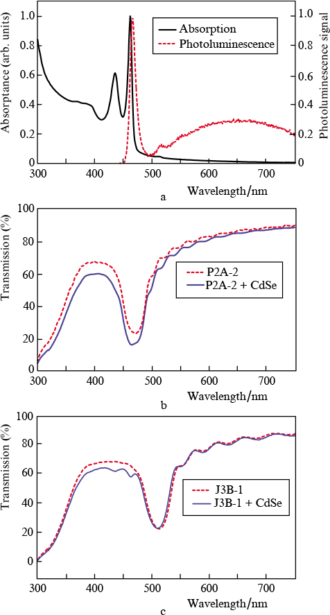
Figure 2. (a) Optical absorption spectrum of a solution of CdSe nanostructures in toluene (solid line) and a characteristic luminescence spectrum of these nanostructures in a photonic-crystal matrix (dashed line), (b) transmission spectra of a sample of photonic crystal P2A-2 without and with CdSe nanostructures (dashed and solid lines, respectively), and (c) similar transmission spectra for a sample of photonic crystal J3B-1.
Download figure:
Standard imageThe transmission spectra of photonic-crystal matrices P2A-2 and J3B-1, processed with a solution of CdSe nanoparticles in toluene (Figs 2b, 2c), are also indicative of incorporation of these nanostructures into the photonic crystal, because the aforementioned spectra exhibit characteristic changes in the ranges corresponding to the excitonic absorption of CdSe nanoparticles. Moreover, sample P2A-2 demonstrates a significant change in the spectral dependence of the photonic stop band, because the stop band position for this crystal is overlapped with the absorption range of CdSe nanoparticles. In turn, for sample J3B-1 with CdSe nanostructures, the form of the stop band remains the same as for the untreated matrix.
In view of the change in the density of photonic states, as well as the selection with respect to the emission direction, the introduction of CdSe nanostructures into a photonic-crystal matrix was expected to allow for control of the luminescence decay dynamics for these objects. This possibility was studied using photonic crystals for which the stop band position matched with the maximum of the photoluminescence spectrum of CdSe nanostructures (P2A-2) or was red-shifted (J3B-1). The results of luminescence kinetics measurements are shown in Fig. 3.

Figure 3. Luminescence decay kinetics of CdSe nanostructures (1) in a photonic-crystal matrix P2A-2, (2) in a photonic-crystal matrix J3B-1, and (3) on a glass substrate.
Download figure:
Standard imageThe relaxation curve in the range from 0 to 5 ns exhibits luminescence kinetics slowdown for the sample of photonic-crystal matrix P2A-2 with CdSe nanostructures [curve (1)], for which the stop-band position coincides with the maximum of interband luminescence of CdSe nanoparticles, in comparison with the luminescence decay for these nanocrystals on glass [curve (3)]. This effect can be explained as follows. When introducing nanoparticles into a photonic-crystal matrix, the particles with sizes smaller than the cavity size will be oriented along the normal to the surface under the electric field induced by photonic-crystal illumination. Apparently, the stop bands acting in certain crystallographic directions (including the normal to the surface) reduce the interaction probability between neighbouring nanoparticles, as a result of which curve (1) in Fig. 3 is located maximally close to the natural decay curve (or even corresponds to delayed kinetics, because the luminescence in the normal direction is suppressed by the stop band), whereas concentration quenching occurs in other samples, which leads to enhancement in the initial portion (0 – 5 ns) and slowdown in the final stage. In the case of sample J3B-1 [Fig. 3, curve (2)], the influence of the stop band is insignificant; the particles are not reliably isolated from each other, and the initial portion of the decay curve is similar to that for nanocrystals on glass.
Apparently, this hypothesis could be confirmed more reliably by measuring time-resolved luminescence spectra with different time windows: in the initial and intermediate decay portions. The ordered orientation of anisotropic particles in a photonic crystal, as well as the electric-field control of their orientation [19] and luminescence properties [20] open up wide possibilities for developing new optoelectronic devices.
4. Conclusions
Samples of inverted photonic-crystal films containing planar and rolled-up (in the form of scrolls) CdSe nanocrystals were prepared and investigated. Based on the transmission spectra of samples treated and untreated with a colloidal solution of CdSe nanostructures, it was concluded that nanoparticles were incorporated into the photonic-crystal films under study. It was demonstrated that the photonic-crystal matrix affects significantly the photoluminescence decay of CdSe nanoparticles. For example, when the position of photonic-crystal stop band is matched with the luminescence peak of CdSe nanostructures, the luminescence decay is slower in the initial stage as compared with the CdSe nanostructures located on a glass substrate; this difference is due to both the influence of photonic-crystal stop band and the concentration quenching weakening. The results or our study demonstrate a possibility of controlling luminescence characteristics of planar and rolled-up nanocrystals by incorporating them into a photonic-crystal matrix, which may be interesting for potential optoelectronic applications.
Acknowledgements
This work was supported by the Russian Foundation for Basic Research [Grant Nos 18-02-00653 a (spectral measurements), 18-02-00811 a (kinetic measurements), and 19-03-00481 a (synthesis of CdSe nanostructures)].