
Abstract
We describe a conductance-based biosensor that exploits DNA-mediated long-range electron transport for the label-free and direct electrical detection of DNA hybridization. This biosensor platform comprises an array of vertical nano-gap biosensors made of gold and fabricated through standard photolithography combined with focused ion beam lithography. The nano-gap walls are covalently modified with short, anti-symmetric thiolated DNA probes, which are terminated by 19 bases complementary to both the ends of a target DNA strand. The nano-gaps are separated by a distance of 50nm, which was adjusted to fit the length of the DNA target plus the DNA probes. The hybridization of the target DNA closes the gap circuit in a switch on/off fashion, in such a way that it is readily detected by an increase in the current after nano-gap closure. The nano-biosensor shows high specificity in the discrimination of base-pair mismatching and does not require signal indicators or enhancing molecules. The design of the biosensor platform is applicable for multiplexed detection in a straightforward manner. The platform is well-suited to mass production, point-of-care diagnostics, and wide-scale DNA analysis applications.
Export citation and abstract BibTeX RIS
1. Introduction
The emergence of nano-biotechnologies is expected to radically improve the current state-of-the art in DNA analysis, and consequently in all related applications. Recent years have witnessed the rapid and continuous growth of this field. Nano-based platforms, and electrochemical analysis tools, are the focus of intense research efforts devoted to the development of new methodologies for the detection of DNA hybridization, and analysis of DNA sequences. The inspiring idea is that nano-probes, and innovative custom-tailored nano-materials, can boost the state-of-the art in DNA analysis—and in the field of biosensors in general—by reducing the costs in terms of sample amount, time and human resources, while maintaining the same sensitivity and specificity as the existing approaches.
Electrochemical-based transduction, which offers low-cost and portable devices, has long been pursued as an attractive alternative to overcoming the drawbacks of current detection assays. Approaches based on the direct electrochemistry of DNA showed limitations early on as a result of interferences from high background signals (Wang 2000). While biosensor strategies based on DNA electro-activity were revealing in their ineffectiveness, the promising results of preliminary experiments claiming the possibility of long-distance DNA-mediated chemistry (Murphy et al 1993, Lewis et al 1997, Arkin et al 1996, Barton 1998) brought about much interest in the original hypothesis formulated by Eley and Spivey (Spivey 1961). This hypothesis postulated π-electron conductivity along the stacking of DNA bases, piled like coins along the axis of the helix and separated by an inter-plane spacing of 3.4 Å, which is a very similar distance to that of graphite.
The hypothesis, of general interest for molecular electronic applications, led to extensive research to reveal the mechanism for long-range charge transfer (Delaney and Barton 2003) and transport (Endres et al 2004) in the DNA molecule. Despite research efforts over the last three decades, the properties and the mechanism of charge migration along DNA are still a subject of debate, animated by contradictory experimental results. Apart from the continued intrinsic difficulties in achieving an effective contact at the electrode/bio-receptor interface, thus hindering direct contact measurements (Hipps 2001), the variability of results has also been attributed to the differences between the experiments performed, and the sensitivity of long-range DNA transport to environmental factors.
While high electron transfer rates have been measured in the context of electron transfer experiments (Murphy et al 1993, Lewis et al 1997), the results from those devoted to electron transport, aimed at determining the conductivity of the molecule, have showed extensive inconsistencies. Different authors have obtained conductivity values ranging from insulator (Storm et al 2001, Zhang et al 2002), wide-band semiconductor (Porath et al 2000) or ohmic behavior (Cai et al 2000). In addition, an induced superconductor characteristic has also been reported (Kasumov et al 2001).
However, biosensor platforms that lie on long-range DNA-mediated charge transfers have been successfully developed and show the capacity to discriminate mismatches and protein binding (Kelley et al 1999, Slinker et al 2011). In these platforms, charge donors and/or acceptors are intercalated in DNA duplexes and the rate of electron transfer is determined by electrochemical analysis. Long-range DNA-mediated electron transfer combined with various labels, including metallic (Barton et al 2011) or anionic (anthrax-quinone-disulphonic acid, AQDS ((Wong and Gooding 2003) and 2-anthra-quinone mono-sulphonic acid (AQMS) (Wong et al 2005)) intercalators, linked-enzymes (Gupta and Atanassov 2011), and DNA groove binders (Johnston et al 1995), have also been previously considered.
Here we present a novel nano-biosensor device based on DNA-mediated long-range electron transport rather than electron transfer. This device, which does not require the use of further signal indicators or enhancing molecules, allows the detection of DNA hybridization and single nucleotide mutation by means of a nano-gap and direct electrical detection. Constituted by an array of gold nano-gap sensors on a Silicon On Insulator (SOI) wafer, the platform has the advantage that it shrinks the size of the probe to that of the molecules involved, a process known to lead inherently to the amplification of the signal-to-noise ratio (Nair and Alam 2006, 2008). DNA detection is achieved through the measurement of the I–V characteristics of the modified nano-gap biosensors, determined before and after the selective hybridization of the DNA target with the functionalized nano-gaps.
The biosensor is achieved by covalently immobilizing two short anti-symmetric ssDNA capture probes on the vertical walls of the biosensor nano-gaps. Both ends of the immobilized bio-receptors are terminated by 19 base pairs, which are complementary to the two terminals of the oligonucleotide target. The biosensor nano-gaps are in this way connected by the specific and selective DNA base-pair interactions, so that the hybridization event is detected by an increase in the nano-gap current. The connection of a gap between two gold electrodes through specific hybridization base pairing was first explored by Braun et al (1998) as an approach to fabricate conductive silver nanowires using DNA as a template.
A scheme of the platform developed here is shown in figure 1.
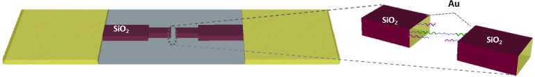
Figure 1. Characteristics of the device. Scheme of an individual device; the gold pads for connecting the source meter unit (SMU) are separated by a bridge covered with 45 nm of SiO2. The middle of the bridge holds the gold nano-metric gaps where DNA capture probes are first immobilized and then hybridized to a target, which is end-to-end complementary to the capture probes.
Download figure:
Standard image High-resolution image2. Experimental results
2.1. Reagents
DNA samples were purchased from Sigma Aldrich, St Louis, MO. The oligonucleotides used are listed in table 1.
Table 1. List of the oligonucleotides used to assemble the device. The mutated probes P23SHMut and P15SHMut have one base mismatch in the fifth position (bold letter in the table) starting from the 5' and 3' ends, respectively.
| Name | Sequence | Length (ss) | % GC |
|---|---|---|---|
| P23SH | 5'-CTTGAGGAGACGGAACGAAGG GCGTGAAGTGGTGAGGAGTGG TGAAGTGCGGG-3'Thiol (C3-S-S) | 53-mer | 60 |
| P15SH | 5'-Thiol (C6-S-S)- GGGCGTGAAGTGGTGAGGAGT GGTGAAGTGCGGGCGTCCAGACCGACTGAGCC-3' | 53-mer | 66 |
| TW | 5'-TTCGTTCCGTCTCCTCAAG GGGAAGGCGCGAAGGTGCGT GAGGAAGTGAAGGCGTGAAG GCGTGTGAAGGCGGTGGTGC GAAGAGAAGGGGGCTCAGTCGGTCTGGACG-3' | 109-mer | 62 |
Sodium phosphate, sodium citrate, sodium chlorite, magnesium chlorite, ethylene-diamine-tetra-acetic acid (EDTA), tris(hydroxymethyl)aminomethane hydrochloride (TRIS) buffer, TritonTM and 6-mercapto-1-hexanol (MCH, purity 97%) were all purchased from Sigma Aldrich, St. Louis, MO.
2.2. Fabrication of nano-gap array
The array of gold nano-gap sensors was fabricated through standard photolithography on a SOI wafer metalized by 10 nm of titanium and 70 nm of gold. The image reversal photoresist, AZ5214, was spin-coated following the three-step protocol provided by the supplier (Clariant GmbH-Germany). It was then exposed to UV light through a chromium mask in the Mask Aligner MJB, SUSS Microtec, with an intensity of 26.5 mWcm−2 for 7.2 s. The time and intensity of exposure were adjusted by considering the loss of power caused by the interposing materials. The wafer was then immersed for 25 s in the AZ develop, following standards. The non-patterned gold was wet-etched at a rate of 2.8 nms−1 by immersing the substrate in gold etchant, Type TFA (Transene Company, inc. Danvers). Thereafter, the titanium was dry-etched by means of a reactive ion etching (RIE) system (at a pressure of 40 mTor, 1 min of CHF3 to oxidize the titanium at a flux of 50 standard cubic centimeter per minute (sccm), followed by 5 min of Cl2 to pull out the oxidized titanium). The last step involved the withdrawal of the protective resist by immersing the sample in AZ 100 remover for about 1 min. The biosensor is then passivated under a SiO2 layer with the exception of the pads, which were uncovered for the application and detection of current. The thickness of SiO2 layer, characterized by ellipsometry, was about 45 nm. All the gold wiring, with the exception of the pads, was passivated to prevent the immobilization of the molecules outside the gap. Next, the gold nano-gaps—with sizes varying from 50 to 60 nm—were milled on the pattern by focused ion beam (FIB) lithography, using a FIB of Ga+ from a Strata DB235 FEI FIB/SEM, operating at an accelerating voltage of 30 kV. As a result, two opposite gold surfaces (approximately 3.73 μm wide and 70 nm high) were created after FIB milling, distanced from each other by about 50 nm. The nano-gap platform was then cleaned in oxygen plasma to remove any organic residuals from the fabrication process. Prior to electrical characterization, the array was also subjected to ozone for 5 min, using a UV-ozone ProCleaner photoreactor from bioforce nanoscience. This treatment was applied to enhance the hydrophilicity of the gap and thus facilitate entry of the solutions. In fact, the UV-ozone treatment induces a hydrophilic state on SiO2 through the formation of OH groups on its surface.
2.3. Assembly of the DNA sensor
Sensor oligonucleotides are assembled at the electrode gold surface by exploiting the affinity of the thiol group for gold atoms. This process gives rise to self-assembling monolayers that are robust against desorption, oxidation, and reduction over a wide range of potentials. To achieve this, a solution comprising 0.05 μM of P23SH, P15SH and 0.45 μM of MCH, for spacing the strands P23SH and P15SH, in 10 mM of TRIS, 1 M of NaCl, 5 mM of MgCl2, and 1 mM of EDTA at pH 7.5 was added to the nano-gap sensor, which was left to incubate overnight. The modified nano-gaps were then thoroughly rinsed and dried with N2 to remove the non-attached probes before electrical measurements were performed.
Afterward, 1 μM of the target sequence in the hybridization buffer (250 mM of sodium phosphate, 15 mM of sodium citrate, 150 mM of NaCl, 1 mM of EDTA and 0.02 mM of Triton at pH 7.42) was deposited on the electrodes and left to incubate for 1 h. The probe molecules were chosen in such a way that they shared 19 complementary bases respectively at the 5' and 3' ends with the target DNA. According to this scheme, the onset of hybridization corresponds to the switching off of the electrical circuit of the nano-gap, which is followed by an increase in gap current. On the contrary, in order to demonstrate the selectivity of the hybridization detection by means of long-range electron transport, the mutated probe oligonucleotides were chosen so as to have single-base mismatch.
2.4. Electrical measurements
Electrical measurements were performed in room atmospheric conditions (referred to as the out of solution environment, with an average temperature of 24 ± 1 °C and 55% relative humidity, r.h.) using a Keithley sub-femtoAmp remote source meter, Model 6430 (Keithley inc.) connected to a probe station. This source meter combines a stable DC power supply in a high-impedance multimeter and a remote amplifier for the measurements of ultra-low current with a resolution of 0.4 fA. Data were registered on a PC work station connected to the femto-ammeter through a general purpose interface bus (GPIB) and were plotted in real-time using Labtracer software (www.keithely.com). To perform the measurements, the two sensor pads were connected to the terminal probes of the SMU.

Figure 2. Results of the fabrication process, a nano-gap shown at different magnifications and an SEM picture of one of the devices used, before and after the hybridization of the target DNA (c) and (d).
Download figure:
Standard image High-resolution imageElectrical measurements in solution were performed using double deionized water, purified with the Millipore A10 Q-gard 1 system (18.2 MΩ cm−1 at 25 °C) and autoclaved. In order to fill the gap with the liquid, a drop of water was delivered to the region between the two gold pads by means of a syringe.
2.5. Scanning electron microscopy (SEM) characterization
Imaging of the nano-gap biosensor was performed with a field emission microscope NOVA NANOSEM 230 by FEI, operating at an accelerating voltage of 10 kV. Empty nano-gaps were characterized before the electrical measurements, and their sizes were evaluated using the image J free-software. DNA-bridged nano-gaps were characterized after the electrical measurements. We must draw attention to the fact that it is difficult to accomplish this characterization without affecting the properties of the trapped DNA, and that in most cases, the functionalized nano-gaps burned out during continuous imaging.
3. Result and discussion
3.1. Sensor nano-gap fabrication
The array patterning was achieved by standard optical photolithography. Afterward, the sensing area was passivated by sputtering 45 nm of SiO2, and the nano-gaps were milled by FIB lithography. The nano-gaps were connected to larger gold pads, thereby allowing a stable electrical connection to the SMU, which permits dc current measurements with femto-ampere sensitivity. The results of the biosensor fabrication process were characterized by means of optical microscopy (figure 2), and SEM was used to establish the nano-gap sizes resulting after FIB lithography (figures 2(b)–(d)). The effective size, averaged over 40 gaps, was 52.02 ± 5.90 nm wide and the gold electrode surfaces confronted in the gap were 3.73 ± 0.23 μm long (with an error of 1σ), and about 70 nm high, which results in a total height of 125 nm considering also the thickness of the SiO2 layer, and the titanium layer (10 nm) under the gold. SEM analysis was also performed in order to confirm the result of the immobilization of the bio-receptors and of the target hybridization process. Figure 2(d) shows bundles of DNA connecting both sides of the nano-gap—thereby allowing the transport of charge between the electrodes—compared to the unconnected gap observed before hybridization (figure 2(c)).
3.2. Direct electrical detection of DNA hybridization and mismatches
Prior to the immobilization of the bio-receptors, we determined the I–V characteristics of the bare nano-gaps, in solution and out of solution, in order to establish the background current. Measurements in solution were done by manually filling the gaps with autoclaved MilliQ (18 MΩ at 25 °C) water, while out of solution measurements were performed under standard laboratory conditions (T = 25 °C ± 1 °C, 55% r.h.). In the case of the DNA molecule, the contribution of the environment to conductivity has been stressed in the literature.
The voltage range applied [−0.8 V; +0.8 V] was chosen to exclude the contribution of the counterions to the measurements (Xu et al 2004). In addition, to exclude the influence of polarization phenomena, we verified the independence of the I–V characteristics from the voltage sweeps. Voltages included in this range are also well-suited to prevent the breakdown of air molecules in the inter-electrode gap region and the reorganization of the electrodes, which can result in a larger gap (Armitage et al 2003).
The nano-gaps were selected for the subsequent functionalization on the basis of the I–V characteristics determined. Only nano-gaps with high resistance values were used. The appearance of hydrophilicity, induced by the UV-ozone treatment, has been associated with a net decrease in the resistance of empty nano-gaps. After some hours of treatment, it has been reported that resistance values recover to those registered before the UV-ozone process (Welch et al 2011), and the nano-gap is viable for low current measurements. In our case, the electrical measurements were always performed the day after this treatment, as the immobilization of the capture probe requires incubation overnight.
Bare nano-gaps and nano-gaps modified with DNA-thiol-probes (P23SH and P15SH, synthetic 53-mer, with 60% of G:C and 66% of G:C, respectively) produced almost the same electrical signal.

Figure 3. I–V characteristics of the devices out of solution. Detection of DNA hybridization under complementary and mismatched conditions. In the inlet the response at 0.6 V.
Download figure:
Standard image High-resolution imageThe difference between these signals is shown as the baseline in the plot (see figure 3). This normalization was adopted in order to take account of the errors introduced by differences in the nano-gap features. In the same graph, we also show the measurements obtained after 1 h of incubation with the well-matched target segment (matched TW, synthetic 109-mer, with 62 % of G:C) and the same sequence hybridized at mismatched DNA-Thiol-Probes (mismatched; P23SHmut and P15SHmut, synthetic 53-mer, with 58.5% and 64.2 % of G:C, respectively). The signals were normalized as before.
We observed a clear increase in current after hybridization of the well-matched DNA target. At the highest positive voltage applied, we measured a current of 125 ± 23 nA, corresponding to a charge migration of 8 × 10¹¹ e−s−1, which accounts for a 98% increase in the nano-gap current after hybridization of the target. On the other hand, the hybridization occurring between the target and the single-base mismatched probes generated 22.8 ± 0.3 nA, which represents a reduction of about 82% with respect to the complementary signal, thus showing a highly selective response of the biosensor developed.
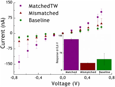
Figure 4. I–V characteristics of the devices in solution. Detection of DNA hybridization under complementary (matched) and mismatched conditions. In the inlet the response at 0.6 V.
Download figure:
Standard image High-resolution imageIn the case of in solution measurements (figure 4), although the maximum current after hybridization of the complementary target was very similar to that measured out of solution (135 ± 30 nA), the relative increment accounted for only 65% of the baseline signal and for 52% in case of the mismatched sequence. The higher contribution of the background in solution therefore leads to a reduction of the sensitivity of the nano-gap biosensor.
The results obtained are in global agreement with those reported in electron transfer-based electrochemical platforms, thus confirming the peculiar sensitivity of DNA-mediated charge migration to single-base mismatches (Slinker et al 2011). In that study, the authors found that a single mismatch in a 100-mer chain gave rise to a shift in the cathodic and anodic peaks of cyclic voltammetry, corresponding to a decrease of almost 47% and 50% of the well-matched signal, respectively.
Despite the standing controversy, there is common concern about the mechanism involved in long-range electron transport along DNA. Accordingly, the charges hop through G:C sites with hop lengths determined by the distance between neighboring bases. The large influence of the sequence details (Lewis et al 1997) have been explained by assuming that hops arise through tunneling in the region containing a maximum of four A-T bridges, and that thermal activation occurs over longer distances (Bixon and Jortner 2000, 2001, Grozema et al 2000).
Table 2. Resistance and corresponding resistivity calculated for the linear part (in the range ± 0.4 V) of the I–V characteristics of the nano-gaps.
| Signal | R (in) (MΩ) | R (out)(MΩ) | ρ (in) (Ω cm) | ρ (out) (Ω cm) |
|---|---|---|---|---|
| Baseline | 30 | 3000 | — | — |
| Mismatched | 20 | 500 | — | — |
| Matched TW | 9 | 20 | 0.7 | 1.5 |
Although it is clear that the sensing principle on which our platform is based is long-range electron transport along DNA, it should be noted that it is difficult to reach a quantitative conclusion about the absolute conductivities that can be associated, without ambiguity, to a given detected sequence. First of all, we worked well above the single molecule device limit. The SEM analysis in figure 2(d) shows that bundles of hybridized DNA, rather than single molecules, are most likely to be trapped inside the nano-gap biosensor. From this analysis, we postulate that the hybridization of the complementary strand inside the nano-gap can also take place through the formation of cross-linked patterns. In the DNA bundles observed with the SEM, we measured a lateral length of about 200 nm, which is greater than the cross-section value of a DNA molecule. In this case, it is expected that the intra-molecular interactions also play a relevant role, contributing to the charge transport through the DNA bridge created, since ssDNA has been reported to support only weak currents (Roy et al 2008).
It is in general not trivial to establish the exact conduction mechanism for the experimental molecular I–V characteristics, especially in the absence of variable temperature-dependent data or molecular length-dependent data; however, this is beyond the scope of this work. Nevertheless, we can extrapolate quantitative information from the linear part of the I–V characteristics (low bias range ± 0.4 V), where the linear Ohm model applies, as it is commonly done in the absence of temperature, and length-variable data (Choi et al 2010, Iqbal et al 2005). By assuming a value of 400 nm2 for the contact area and a nano-gap length of 52.02 ± 5.90 nm (on the basis of the SEM characterization of figures 2(b) and (d)), we estimated the corresponding resistivity values (table 2).
These values should be interpreted as upper limit to the real molecular resistivity because they also include the contact resistance. Indeed, it is clear from the I–V characteristics that the three signals separate better at higher, than at lower voltages.
The calculated values are in general agreement with those reported for similar platforms. Using STM analysis, a resistivity of 1 Ωcm was found for a poly(dG)-poly(dC) of 50 nm of self-assembled DNA networks (Cai et al 2000). Wang (2008) reported a value of about 2 Ωm by ac impedance measurements on a random λ DNA bundle 20 nm in width and 25–30 nm in height, while for a 15-mer sequence bridging a carbon nanotube gap a resistance of 1 MΩ was observed (Guo et al 2008). This value increased to 25−40 GΩ when an 80-mer sequence bridged a carbon nanotube (Roy et al 2008).
We observed that the occurrence of a G–A mismatch on one side, and a G–T mismatch on the opposite one, led to a four-fold increase in the resistance of the mismatched sequence with respect to the fully complementary strand. This increase is attributed to the reduced stability of the hydrogen bond caused by the on-site changing of the ionization potential and the alteration of the π stack structure (Hwang 2011). In metalized DNA (Ni-DNA) (Jagjian et al 2009), where the increase in resistance depends exponentially on the number of mismatches, a G–T mismatch was also found to account for a smaller amount of resistance than a G–A.
3.3. Reusability of the DNA sensor
The wide-scale application of DNA analysis requires the implementation of highly sensitive methods on inexpensive platforms. For this reason, the regeneration of a DNA biosensor is a critical feature. The design of the long-range electron transport (LoRET) biosensor allows assessment of the reusability of the capture probes by simply denaturalizing the hybridized DNA. In order to achieve this, the molecular device was exposed to a solution 10 mM NaOH for 2 min. After extensively washing the array with abundant deionized water and drying it with nitrogen flux, we measured the I–V characteristics of de-hybridized/hybridized gaps during various cycles. The results are shown in figure 5.
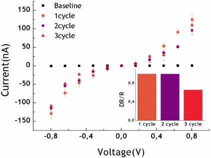
Figure 5. Currents measured after denaturalization and further incubation with the complementary target under out of solution conditions. In the inlet, the relative increment of the nano-gap resistance with respect to the bare gap resistance (baseline), after each denaturalization cycle at 0.8 V.
Download figure:
Standard image High-resolution imageThe decrease in current after the regeneration, which was close to the original value obtained after the gap functionalization with the capture probes, shows the effectiveness of NaOH to break the hydrogen bonds between the bio-receptors and the DNA target. Also, the further increase in current after regeneration, and re-hybridization with the same target, indicates that the bio-receptors were not damaged by the regeneration solution, maintaining their ability for further hybridizations. The designed nano-biosensor platform allows their re-usability, thus reducing the cost of subsequent analysis.
3.4. Quantitative measurements
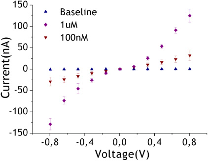
In order to prove the capacity of the biosensor for quantitative measurements, we studied the possible dependence of the nano-gap currents on a range of target concentrations. A current signal trend was observed to be directly proportional to the sample concentration (figure 6). We detected a signal distinguishable from that of the control at a target concentration of 100 nM. This is the lowest detection limit reached compared with existing platforms that rely on long-range electron transfer combined with proper labels (4 μM (Wong and Gooding 2003, Wong et al 2005); 25 μM (Slinker et al 2011)). Only in one study, was an improvement (0.5 nM) of our detection limit achieved, but it should be highlighted that this was a labeled system (Wong and Gooding 2006).
In contrast, in our platform the detection was achieved in a total label- and reagent-free fashion, as it was based solely on the robustness of DNA LoRET. The reusability of the device, up to three cycles, the suppression of the current after the denaturation of DNA, and the subsequent increase after incubation with the target, together with higher currents at higher target concentrations, evidence that the electrical signal measured originates from the DNA hybridized inside the nano-gap biosensors.
Figure 6. Response of the sensor at a range of target TW concentrations (out of solution data are shown).
Download figure:
Standard image High-resolution image
4. Conclusions
Here we demonstrate the feasibility of a conductance-based platform that relies on the electrical properties of DNA for the direct and label-free detection of DNA hybridization and DNA mismatches. This is a proof-of-concept that we believe can be fruitfully explored to develop a novel kind of electronic DNA biosensor with the potential to be simultaneously sensitive, selective, reagent-less, and especially label-free. For well-matched and mismatched targets, it is sufficient to expose the molecular assembled device for 1 h to the solution containing the target oligonucleotides. Shorter incubation times will be tested in future assays in order to reduce the analysis times.
We successfully detected the increase in the nano-gap current in approximately 25% of the devices after incubation with the target sequence. Regarding the rather low statistics, it should be noted that obtaining a reproducible fabrication of nano-gaps and successfully trapping the molecules inside them continue to be a challenge. Given that the capture probes are anti-symmetrical each other, the successful hybridization of the target can be achieved only when the probes are positioned directly in front of each other. We consider that the efficiency of the biosensor could be increased by means of site-selective deposition of the capture probes, which could be achieved using dielectrophoresis.
Our results reveal this new platform to be sensitive (100 nM LOD), selective (one base mismatched clearly detected) and reusable (up to three cycles).
Properly functionalized arrays of nano-gaps can offer a realistic alternative to the traditional geno-sensor arrays, which are based mainly on fluorescence detection methods.
Acknowledgments
This work was financially supported by the OLIGOCODES project (MAT2011-29335-C03-03), funded by the Spanish Ministry of Science and Innovation (MICINN) in the framework of the VI National R&D&i Plan 2008-2011. CIBER-BBN is an initiative funded by the VI National R&D&i Plan 2008-2011, Iniciativa Ingenio 2010, Consolider Program, CIBER Actions and financed by the Instituto de Salud Carlos III with assistance from the European Regional Development Fund. The Nanobioengineering Group has support from the Commission for Universities and Research of the Department of Innovation, Universities, and Enterprise of the Generalitat de Catalunya (2009 SGR 505).