Effect of Doping on the Electrical Characteristics of ZnSe
by
Narsingh Bahadur Singh
1,*, 
Ching-Hua Su
2,
Fow-Sen Choa
1,
Bradley Arnold
1,
Puneet Gill
1,
Charmain Su
1,
Ian Emge
1 and
Rachit Sood
1 1
Department of Computer Science and Electrical Engineering, University of Maryland Baltimore County, 1000 Hilltop Circle, Baltimore, MD 21250, USA
2
EM31, NASA Marshall Space Flight Center, Huntsville, AL 35812, USA
*
Author to whom correspondence should be addressed.
Crystals 2020, 10(7), 551; https://doi.org/10.3390/cryst10070551
Submission received: 14 May 2020
/
Revised: 31 May 2020
/
Accepted: 23 June 2020
/
Published: 27 June 2020
Abstract
:The effect of sulfur, iron, and chromium doping on the electrical characteristics of ZnSe single crystals was studied. The crystals, grown by the physical vapor transport method (PVT) at NASA Marshall Space Flight Center, were characterized by measuring electrical resistivity, capacitance, and dielectric constant using LCR meter. The morphology was studied by scanning electron microscopy to determine the crystallinity and micro defects. The measured resistivity and dielectric constant showed tunability as the function of frequency in the range of 100 Hz to 100,000 Hz, indicating the suitability of doped material for tuning devices. Besides, for the range from 50 mV to 1000mV, there was no difference in values for the studied frequency range, indicating no degradation or breakdown in the material. All doped ZnSe crystals with sulfur, iron, and chromium showed a similar trend as the function of frequency. Cr-ZnSe showed very high resistivity and lower dielectric constant compared to S-ZnSe and Fe-ZnSe crystals.
1. Background
Since past eight decades, binary and ternary selenides, specifically ZnSe, have proven as an excellent multifunctional material for multiple applications, including high power lasers operating in the ranges of mid-wave infrared (MWIR) and long-wave infrared (LWIR), surveillance, windows, hyperspectral imagers, coatings, and environmental monitoring. The pioneering work of Mazelsky et al. [1] demonstrated the feasibility of pulling large crystals of this class of volatile materials. Modified melt growth methods have involved pressurized atmosphere or encapsulation for controlling evaporation and stoichiometry. Since mid-sixties, vapor transport method with and without carrier gases have been developed [2,3,4,5,6] for zinc selenide, which ultimately has turned into a process entitled chemical vapor transport process. However, large ZnSe crystals have been grown by vapor transport method, and attempts have been made to develop to control homogeneity in large crystals by controlling thermal and solutal (impurity) convection during a variety of crystal growth [7,8,9,10,11,12,13] to understand the effect of microgravity. For the ZnSe applications in the area of laser development, two major approaches have been used—(a) utilizing the rare-earth or transition metal-doped bulk single crystals and (b) thick film of ZnSe on lattice-matched substrates entitled as quasi-phase materials (QPM) [14,15]. For both—bulk and QPM approaches—zinc selenide has been proven [16] to be an excellent crystal because of its wide transparency range, low optical absorption, good stability, reasonably high mechanical and polishing characteristics, and high laser damage threshold. Studies to understand the role of convection in doped crystals [8,9,13] have provided insight to develop homogeneously doped crystals and uniform properties. Very similar to optical emissivity and absorption studied extensively for ZnSe crystals [9,10,11,12], the dielectric and resistivity values can throw lights on the quality of ZnSe crystals since the defect density and grain boundaries both contribute significantly to dielectric constant and electrical resistivity. When an electric field is applied in the ZnSe slab, domains are aligned, and atoms shift in the direction of the electric field. This results in polarization due to positive and negative ions shift in their positions. This type of alignment of the domain is greatly affected by the presence of defects and grain boundaries in ZnSe crystal and hence affects the electrical properties. In the doped ZnSe crystals, point defects may increase and cause additional inhomogeneity and hence changes in properties. In this paper, we studied dielectric constant and resistivity of sulfur, iron, and chromium-doped large single ZnSe crystals grown by physical vapor transport method (PVT).
2. Materials and Methods
Pure and doped ZnSe large bulk single crystals were grown at NASA Marshall Space Flight Center by PVT. The details of growth parameters and optical characteristics are discussed in detail in references [8,9,10,11,12] for the sulfur, iron, and chromium-doped ZnSe crystals. All these doped crystals were grown in the same furnace and using an identical growth rate and thermal gradient. Besides, crystal slabs under this study were taken from the same part of the crystals to avoid the difference due to segregation on the seed end or the tail portion of the crystal. These crystals were designated as: (a) S-ZnSe, (b) Fe-ZnSe, and (c) Cr-ZnSe. Since each dopant has different sizes and oxidation states, we expected that defects generated and properties would be different. The concentration of each dopant and its effect is discussed in each section.
2.1. Fabrication of Slabs for Characterization
All doped ZnSe crystals were cut by string saw and polished [11,12] on a parallel surface for detailed characterization. Rough cut surfaces were polished by ethylene glycol (Sigma-Aldrich Chemicals, Saint Louis, MO, USA) and SiC (Sigma-Aldrich Chemicals, Saint Louis, MO, USA). The typical thickness was larger than 5 mm in each case.
2.2. Morphological Studies
The morphology of each crystal was determined by the scanning electron microscope FEI NOVA NANOSEM 450 (FEI, Hillsboro, OR, USA). We used typically a range of 2 to 20 kV energy. The data shown here are for the 2–120 kV. The SEM sensitivity for the concentration determination was limited to 1%. The iron and chromium samples showed some signs of charging, which indicated that there were some traces of metal impurities.
2.3. Electrical Characterization
Parallel polished surfaces were prepared for electrode bonding. We observed that both gold and silver were stable on the ZnSe surface. We placed silver paste similar to that described in reference 24 on parallel surfaces for the electrical contact. Resistivity and capacitance were measured by Hewlett Packard 4284A LCR meter (HP/Agilent, Santa Clara, CA, USA). The following equation was used to determine the dielectric constant. C = εεoA/d, where ε is the dielectric constant of the material, εo = 8.854 × 10⁻¹², A is the overlapping surface area of the plates, d is the distance between the plates, and C is capacitance.
3. Results and Discussion
The surface quality, bulk defects, such as voids, precipitates, and morphology, of all doped crystals were determined to correlate the properties with these parameters. The results of each doped crystal are described in the following sections.
3.1. S-ZnSe Crystal
The doping of the sulfur was performed by mixing ZnS powder in the source ZnSe powder before the crystal growth. Source material with a stoichiometric concentration of ZnSe0.91S0.09 was loaded, and the crystal was grown by physical vapor transport method [7,8,9,10,11,12]. The growth method and details of parameters are described by Su et al. [9,10,11] and have not been discussed here. Similar methods with slight modification in geometry and growth parameters have been used [13,14,15,16,17] for bulk and QPM materials by several investigators. Some other modifications have been used for Fe-doped ZnSe for various applications [18,19,20,21], including mid-IR laser development.
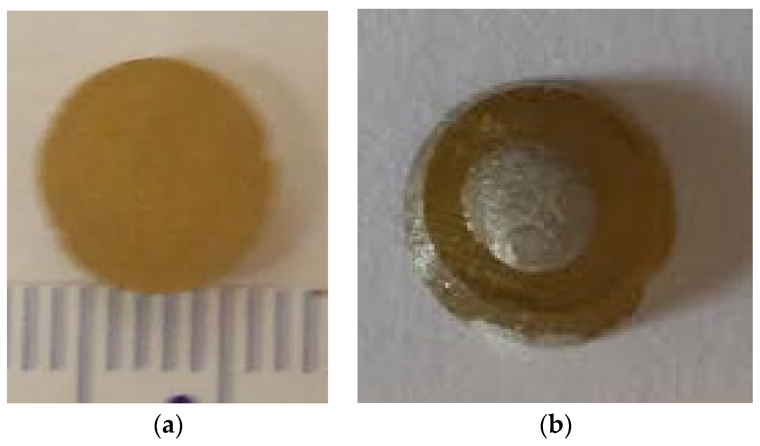
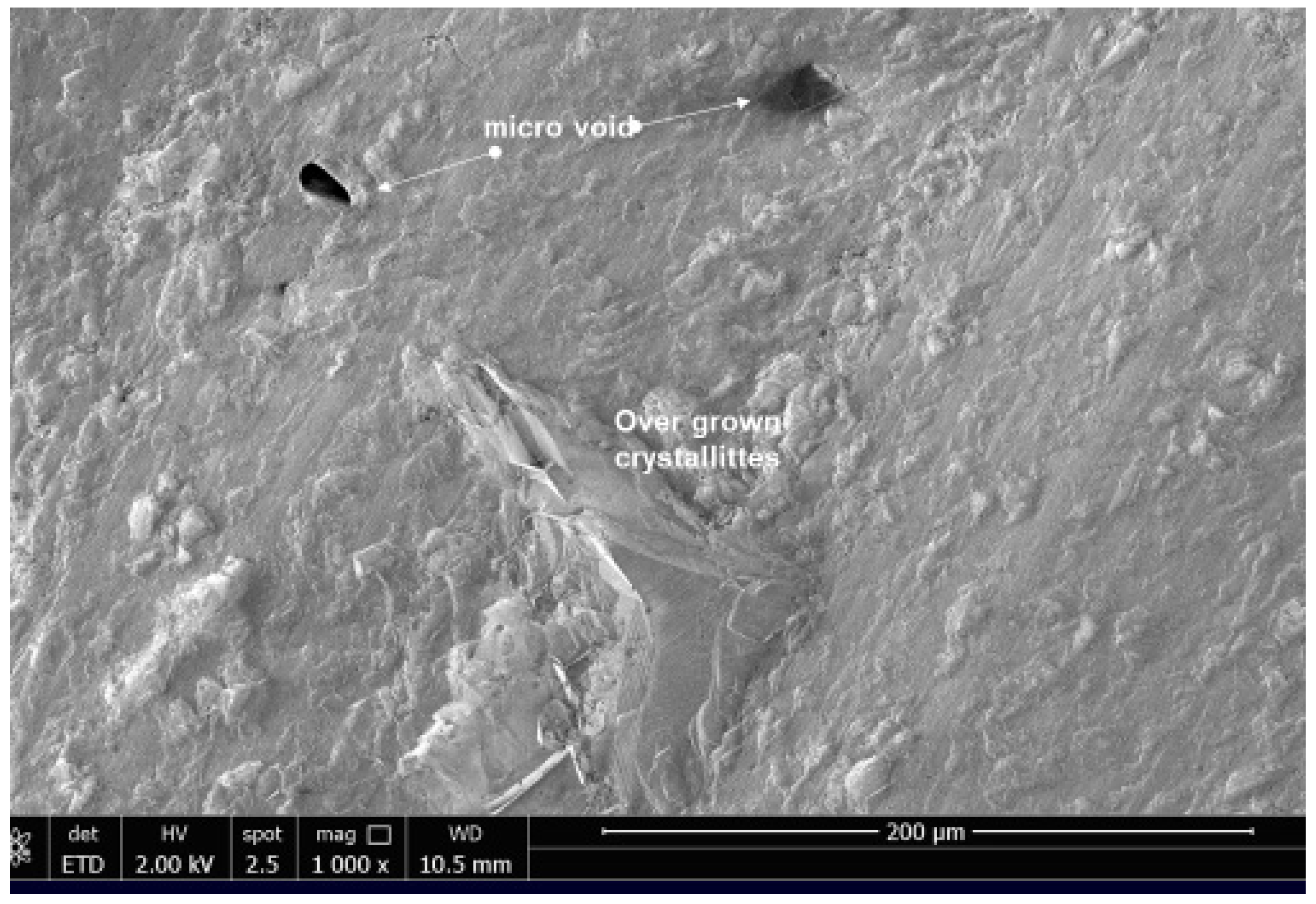
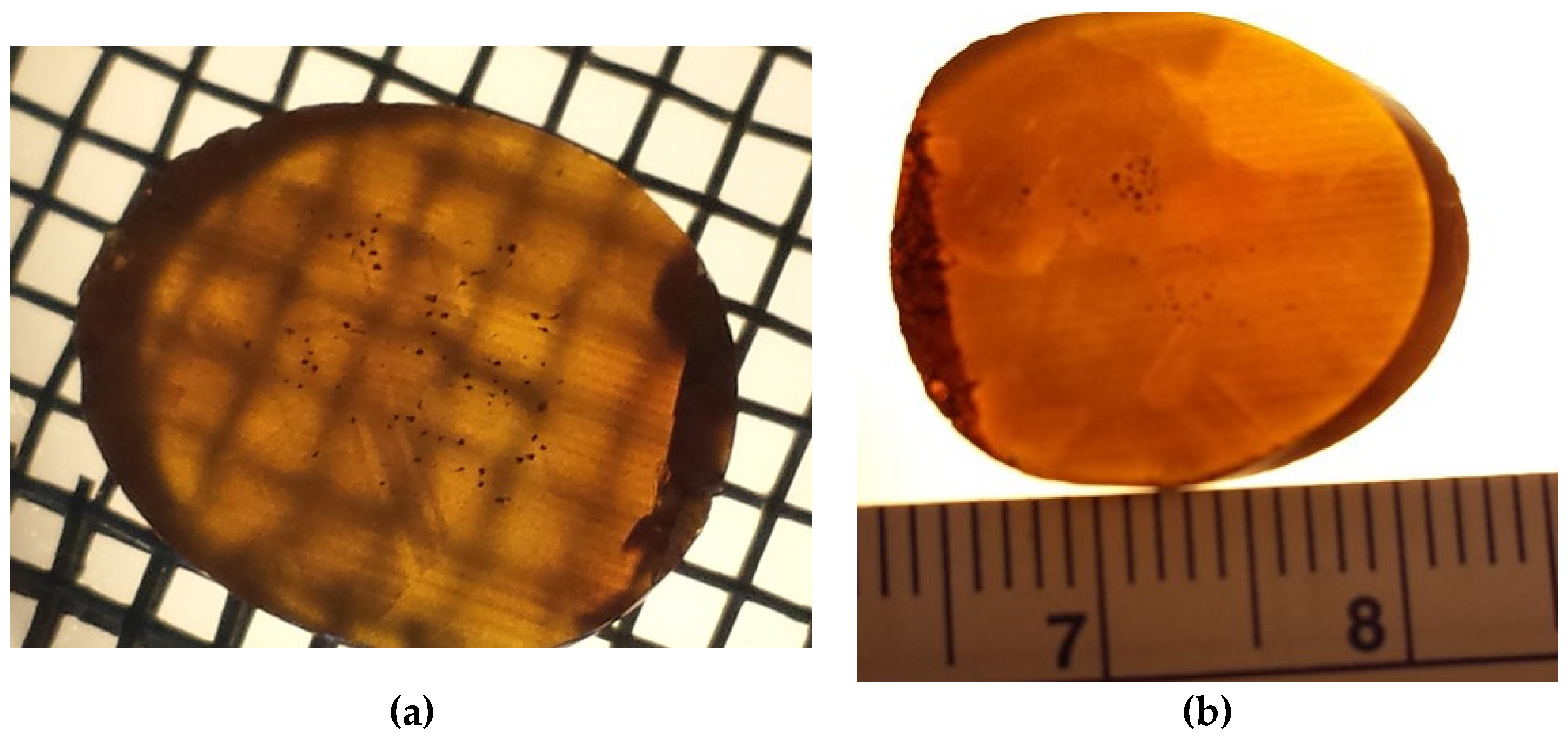
As described previously, the single crystallinity was assessed [11,12] using an X-ray diffractometer equipped with a micro source and a triple-bounce Ge crystal beam conditioner. The sulfur composition determined using the Physical Electronics model 600 scanning Auger equipped with an argon sputter system showed sulfur concentration much lower than doped 0.09 mole fraction. X-ray diffraction study using the current and voltage of 35 mA and 45 kV, respectively, indicated that the sample showed peaks, which shifted to higher angles compared to pure ZnSe and showed a single peak corresponding to (111), indicating good crystallinity. Data are discussed in reference [11] in detail. Figure 1 shows sulfur-doped parallel polished (a) slab and (b) a slab with silver paste on the surface. The silver paste was used as an electrode on both surfaces for electrical measurement. The overall quality of crystal was inferior to pure ZnSe crystals grown by PVT due to a very high sulfur doping, which caused double-diffusive convection as well as point defects. Figure 2 shows the micromorphology of the slab. There were small microvoids and small arrays of line defects in a few regions. This type of morphology was possibly due to changes in the localized deposition rates and incongruent nutrients with different vapor pressure in the growth chamber.
The morphology showed a few small regions free from boundaries. In some portions, there were overgrowth and aggregates, which could be attributed to stresses developed during uneven cooling of large size crystal in the quartz container. Since concentration was extremely small, stress due to differences in the lattice parameters of sulfur and selenium was not likely. The crystallites along the boundaries developed during the cooling of the ampoule and size were in the range of 1–3 micrometers. Within the limit of EDX, we did not observe any changes in the stoichiometry of the ZnSe matrix.
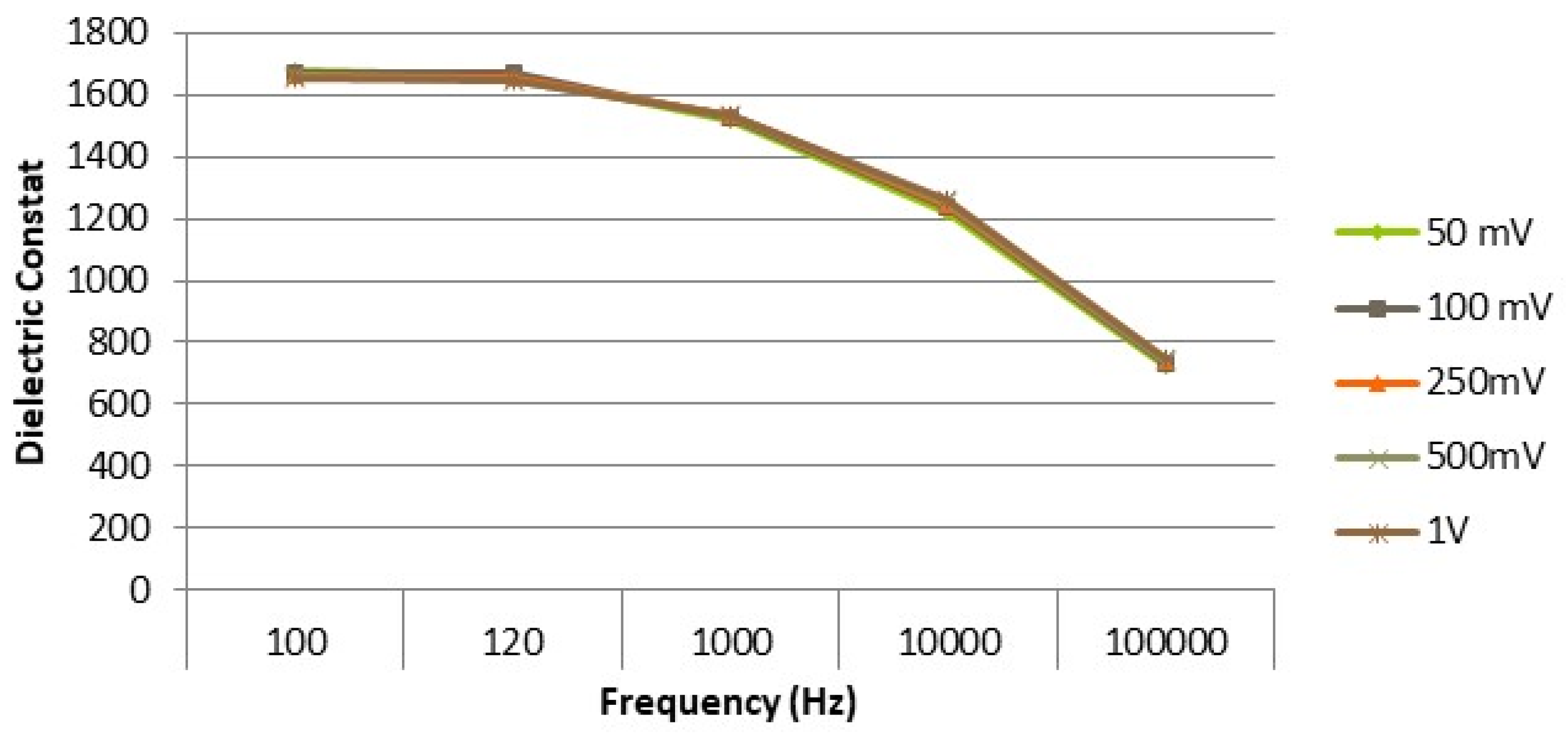
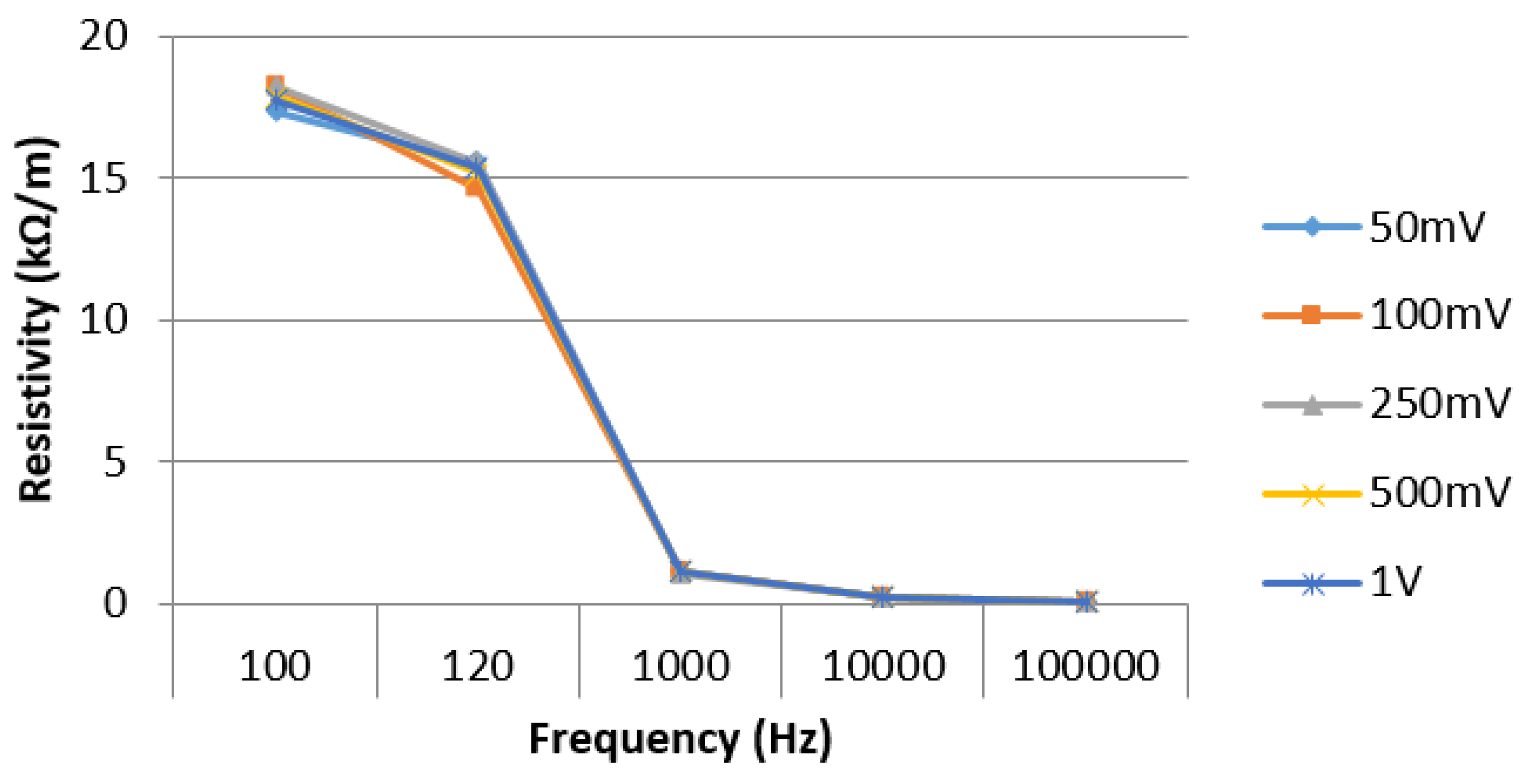
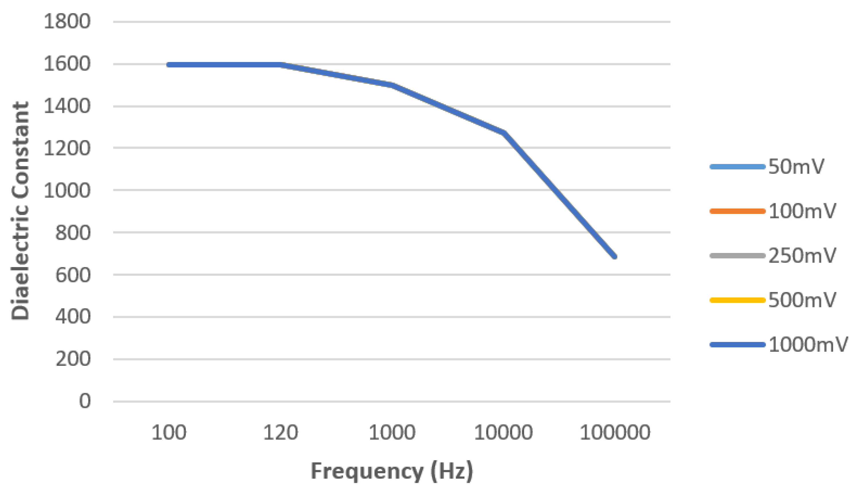
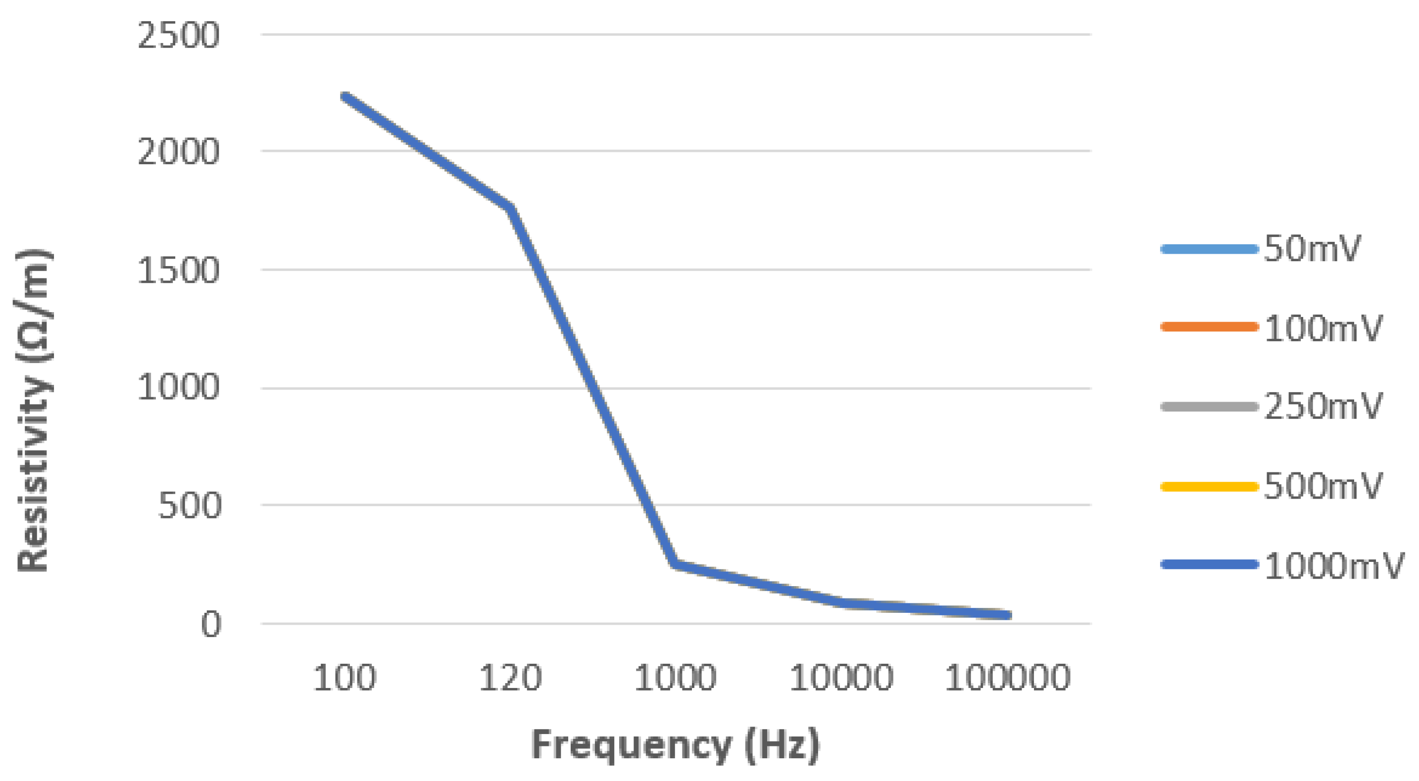
The samples used for the electrical measurements were 1.5 mm thick, and the area of the silver electrode [22] was 2.74 mm2. The data for both resistivity and dielectric constant were determined by measuring resistance and capacitance for the sample. The bias range was 50 mV to 1 V, and the frequency range was 100 kHz to 100,000 kHz. The resistivity and dielectric constant are given in Figure 3 and Figure 4. The dielectric constant and resistivity both decreased with frequency as well as with increasing bias. There was a steep drop in resistivity after 120 Hz. Besides, the values observed were higher compared to values reported for ZnSe powder. Results showed that sulfur-doped crystals could be used for tuning devices, where dielectric constant could be tuned as a function of frequency. Although there was a continuous change in dielectric constant as the function of frequency, for the resistivity, this effect was more effective in lower frequency (100 to 1000 Hz) range.
3.2. Fe-ZnSe
The source material containing iron had a composition of Zn0.96Fe0.04 Se. The iron concentration in the grown crystal, measured by glow discharge mass spectroscopy (GDMS), showed much lower value, and it was in the range of 4.6 × 10⁻⁴ ppm. But even such a low concentration affected the quality of the crystal significantly. Similar to that of sulfur-doped ZnSe crystal, we fabricated Fe+2-doped boules also into thin slabs by cutting and polishing. Good surfaces were achieved by final polishing with silicon carbide slurry and then cleaned with glycol. Figure 5a,b show the optical bulk transparency without and with wire mesh in the background. We determined the bulk homogeneity, inclusions, and distortion by the illumination of the polished crystal disk and did not observe gross defects, such as precipitates or voids, on the polished surfaces or in bulk. There was no sign of striations due to thermal stress or impurities. There were small cracks on the edges of the slab.
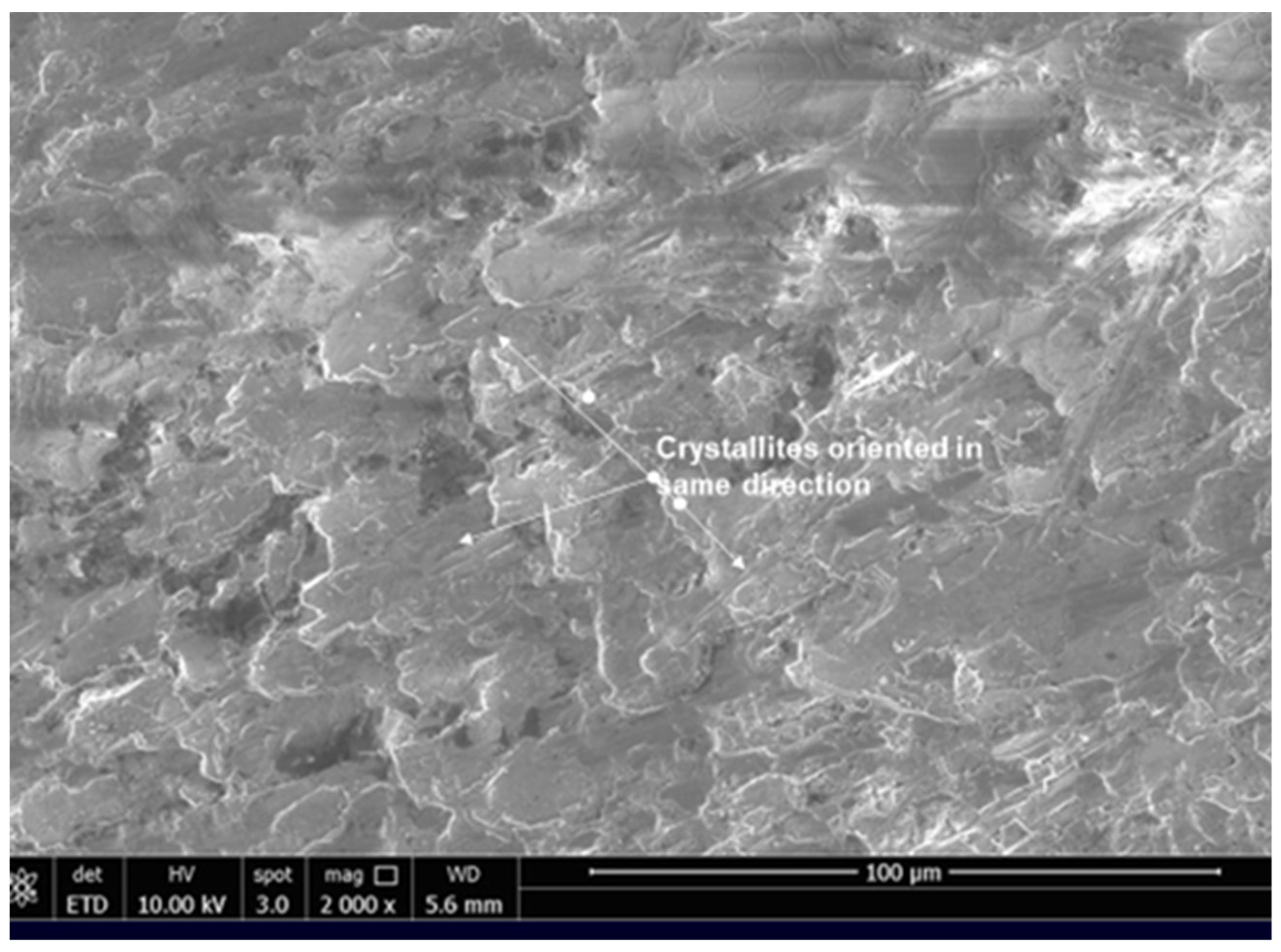
Figure 6 demonstrates the micromorphology of Fe-ZnSe crystals at 10 kV power. The figure shows microfacets and boundaries throughout the crystal. Most of these microcrystalline facets contained textures of the growth patterns. We observed grain boundaries around the textured grains. These types of textures were possible due to the high thermal gradient and uneven cooling of large crystals after the growth. Due to the low thermal conductivity of these semiconductors, surfaces generally cool faster than the bulk portion of the boule. Unlike sulfur-doped crystals, there were no microvoids, microbubbles, and overgrown crystallites in this case. This might be due to a very low concentration of iron compared to sulfur in the source material. The concentration of iron was below the detectivity of the EDX instrument.
Similar to the case of S-ZnSe crystal, measurements for dielectric capacitance and resistance were taken for the bias voltage of 50 mV to 1 Volt and a frequency range of 100 kHz to 100,000 kHz. Figure 7 and Figure 8 show the resistivity and dielectric data. Both data showed a significant change in values of dielectric constant and resistivity as the function of frequency, showing tunability in the material. It showed that iron-doped crystals also could be used for tuning devices, where dielectric constant could be tuned as a function of frequency. The data also showed that there was no effect of voltage on values. Data taken from 50 mV to 1000 mV showed constant value for the dielectric constant, indicating that there was no change in characteristics of material or breakdown due to voltage. A similar observation was observed for the resistivity also for the applied bias voltage.
3.3. Cr-ZnSe
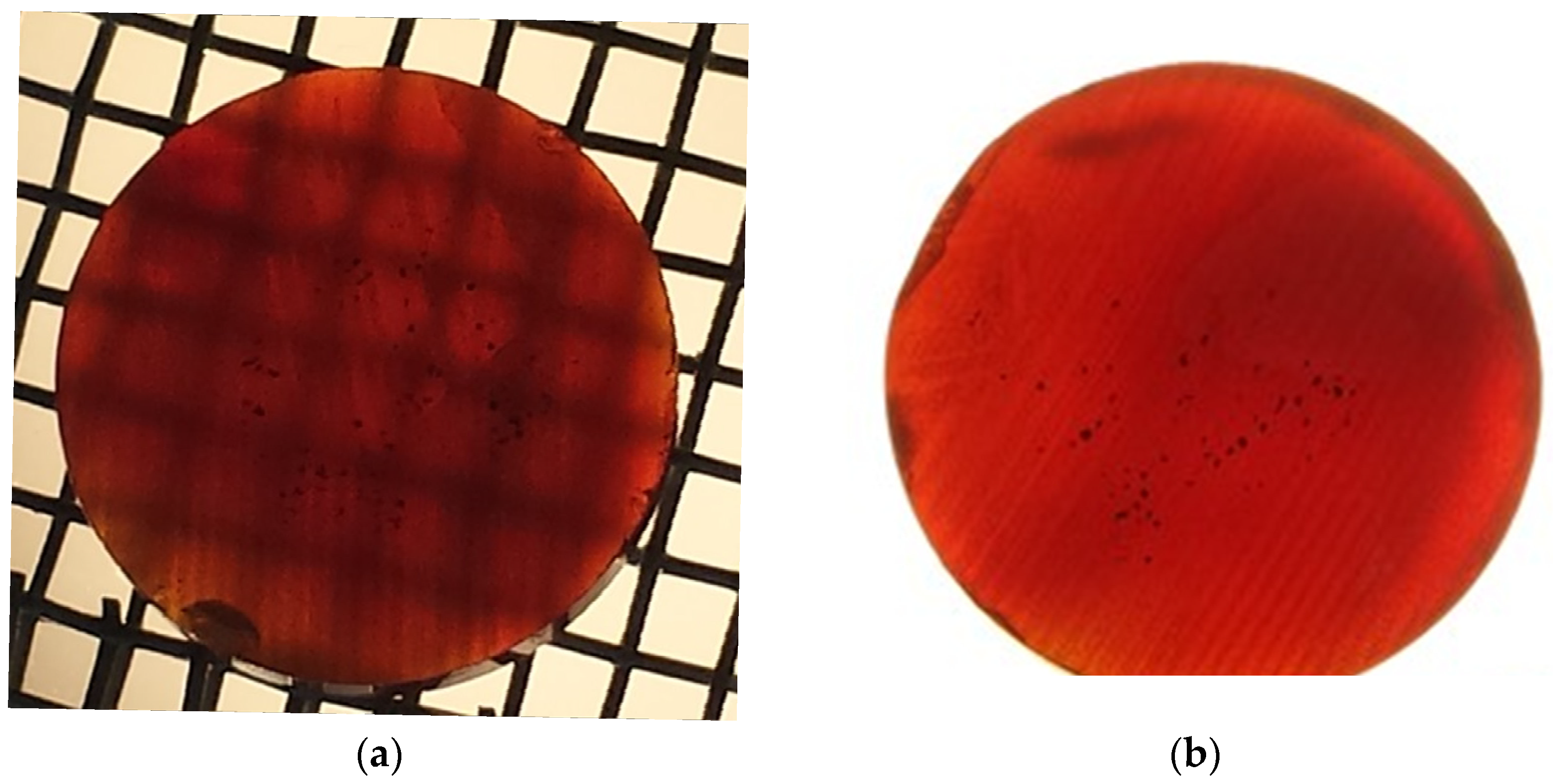
The source material containing chromium was prepared with a composition of Zn0.987Cr0.013Se for crystal growth. The chromium concentration in the PVT grown crystal, measured by glow discharge mass spectroscopy (GDMS), showed a value in the range of 3.2 × 10⁻³ ppm. Similar to the case of sulfur and iron-doped ZnSe crystals, Cr2+-doped boule was also cut and polished into slabs. Figure 9 shows the fabricated Cr-doped ZnSe disks with and without a wire mesh in the background. We did not observe any optical distortion in the crystal slab, and it was transparent. Crystal slab did not show any voids, crack, or precipitate. However, Cr-ZnSe was reddish in color compared to both sulfur and iron-doped ZnSe slabs.
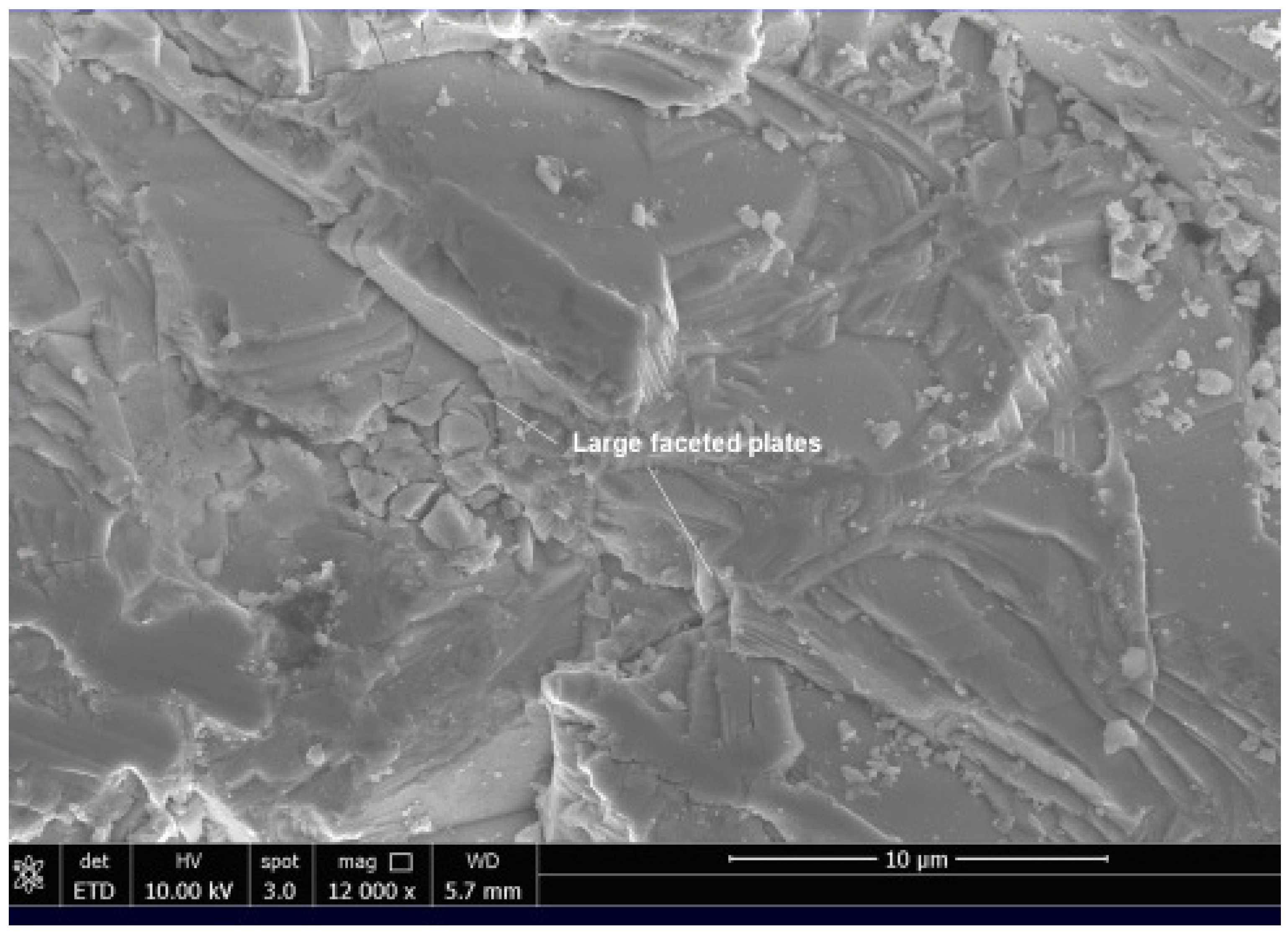
The morphology determined by scanning electron microscope NOVA NANOSEM 450 system at 10 kV is shown in Figure 10 for the Cr-ZnSe crystals. The morphology indicated that Cr-ZnSe crystals had large faceted microplates in bulk. The homogeneity of these plates was not uniform. At some places, there were larger than 5 μm long plates with a thickness of 0.5 μm. Detailed analysis indicated the presence of microcracks. In some portion of the crystal, we observed small crystallites, which were generated by fractured microplates. It was clear that Cr-ZnSe crystal contained more microcracks in bulk. Besides, Cr-doping might have affected the kinetics, and this might be the reason for the faceted morphology. This behavior was not observed in S-ZnSe and Fe-ZnSe bulk micromorphology.
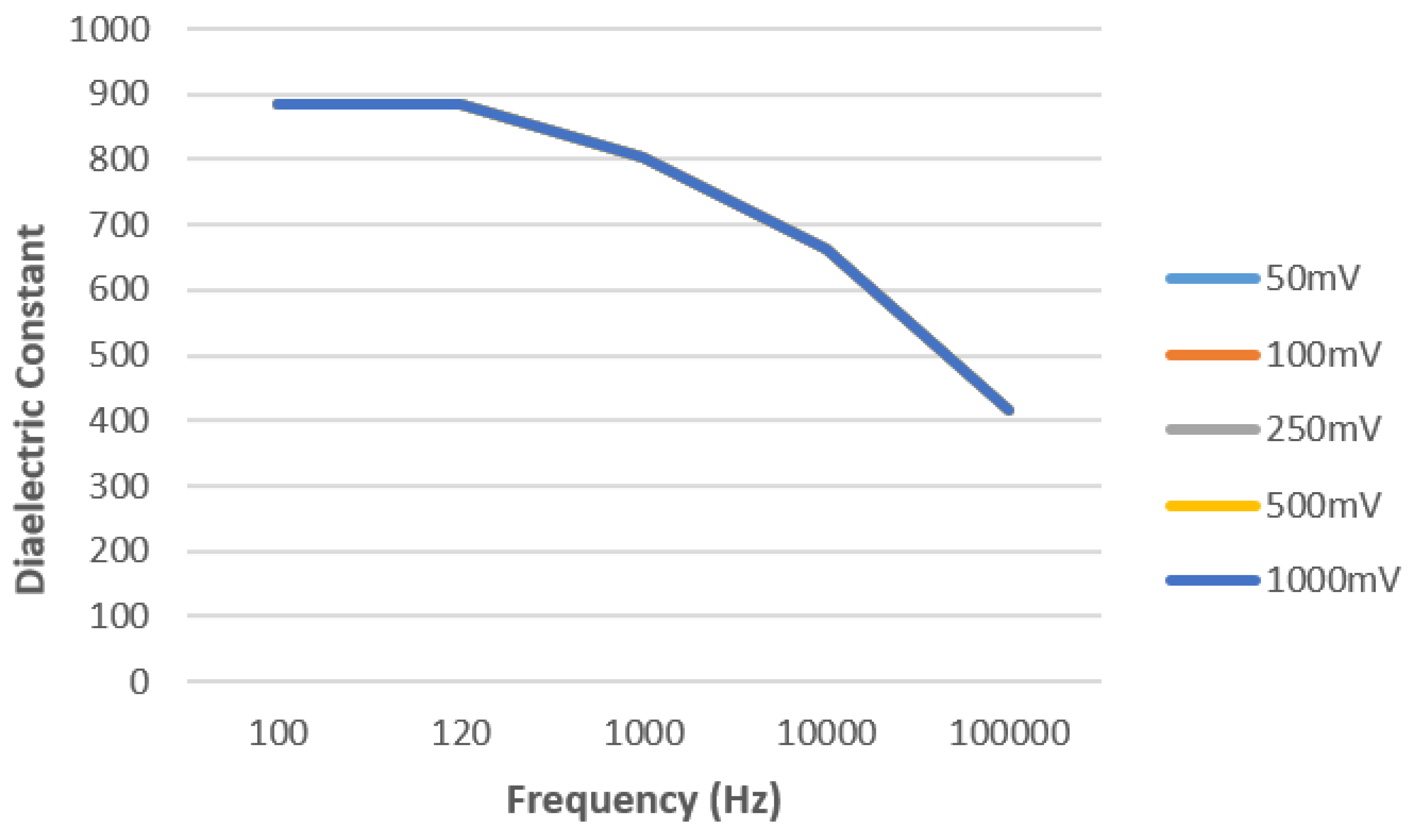
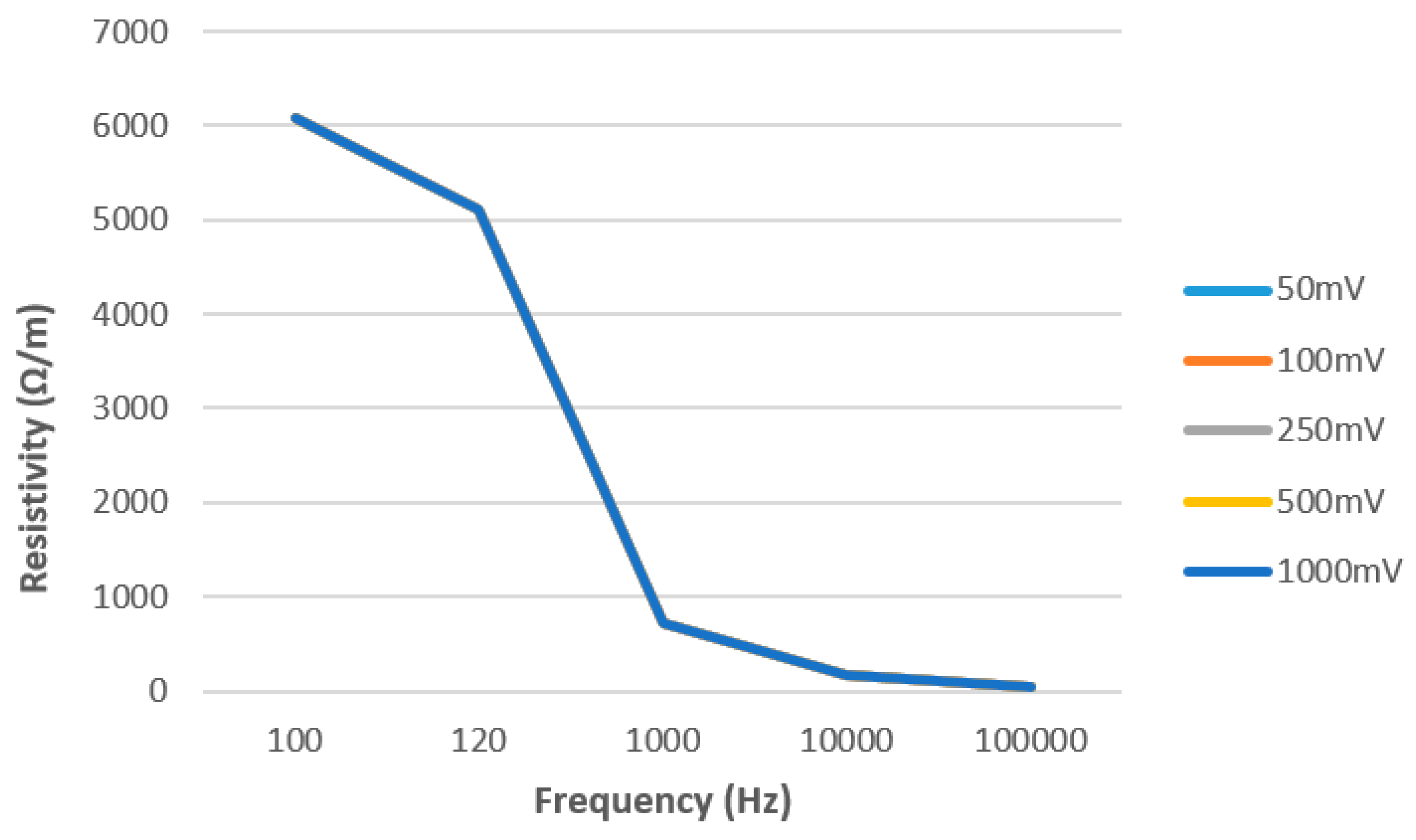
We measured the dielectric capacitance and resistance for Cr-ZnSe crystal similar to the Fe-ZnSe slab for the bias voltage of 50 mV to 1 V and a frequency range of 100 kHz to 100,000 kHz. Figure 11 and Figure 12 show dielectric constant and resistivity data. The data showed a decreasing trend in the dielectric constant and resistivity of the sample as the function of frequency, and the change in values showed dielectric tunability in the material. The values of the dielectric constant for Cr-ZnSe crystal were much lower compared to S-ZnSe and Fe-ZnSe crystals. The resistivity of Cr-ZnSe crystal was almost three times higher than other crystals. This was expected since chromium is a deep level dopant similar to vanadium. Data indicated that a high resistivity ZnSe material could be obtained by chromium doping for very high voltage applications.
4. Conclusions
The effects of sulfur, iron, and chromium doping on the electrical characteristics of ZnSe single crystals were determined. The quality of doped crystals was inferior to that of pure ZnSe due to solutal convection, which had been proven by microgravity experiments. The bulk transparency and morphology were studied by scanning electron microscopy to determine the gross defects, crystallinity, and micro defects. Measured resistivity and dielectric constant for all doped crystals showed tunability as the function of frequency in the range of 100 Hz to 100,000Hz, indicating the application of doped ZnSe as tuning devices. For the bias range of 50 mV to 1000 mV, there was no difference in values for the studied frequency range, which showed no breakdown in the materials. Cr-doped ZnSe had the highest resistivity, indicating its possible applications in very high voltage devices.
Author Contributions
C.-H.S. of NASA Marshall Space Flight Center performed the growth of doped ZnSe crystals at NASA Marshall Space Flight Center. He used Physical Vapor Transport method for the growth of crystals. He participated in writing of manuscript also; F.-S.C. designed the experiment for parallel plate capacitor need and supervised R.S. for determining the dielectric constant from capacitance data. F.-S.C. and N.B.S. analysed optical quality, morphology and dielectric data to evaluate the difference in each sample. They determined that these doped ZinSe samples can be used for a novel tuner devices for variety of RF applications; B.A. guided to design the sample for SEM and electrode bonding before measurements. He supervised I.E. and P.G. for designing the experiments especially design of sample to stop vibration and plate paralelism design during measurements and interpretation of data. B.A. an expert in materials, lasers and laser spectroscopy discussed difference in role of each dopant. He guided to prepare proper concentration of silver paste (solvent) and stability on ZnSe surface to avoid diffusion in the bulk. P.G. and C.S. calibrated LCR meter and collected data for sulfur, iron and chromium doped zinc selenide samles. R.S. also took data and independenly verified. All these three students measured capacitance, resistance and impedance for all samples. P.G. and R.S. analysed the data for all samples. C.S. measured the capacitance, resistance and impedance. She calibrated these data with measured data of PCCTO on the same LCR meter to ensure accuracy of dielctric constant and resistivity. She and P.G. collected experimental data for the dielectric, resistivity and impedance of the sulfur, iron and chromium doped samples. They analysed data with N.B.S. She and P.G. developed the data as function of bias and frequency. I.E. fabricated parallel samples, placed silver electrodes by preparing proper solution/paste of as suppled silver paste for ZnSe surface. I.E. and R.S. determined the stability of silver electrode on doped ZnSe by placing samples up to 50C to determine diffusivity in the bulk. I.E., R.S. and P.G. optimised and collected morphology of all samples with scanning electron microscopy. R.S. took the lead for SEM studies and took data with I.E. and P.G. He independently measured capacitance to determine the calibration of LCR meter. He also helped in evaluating effect of stability of silver paste in ZnSe. He fabricated samples and is continuing to develop ZnSe based QPM structures. He plotted the data for some samples. N.B.S. designed the over all plan for the execution of the project, participatde with students on each task and prepared the manuscript for publication. He was responsible to coordinate with B.A. and F.-S.C. to summarize the findings from the experimental data. All authors have read and agreed to the published version of the manuscript.
Funding
This research was patially funded by NASA/Marshall Space Flight Center through a purchase order for services #80NSSC19P1269.
Acknowledgments
The authors would like to acknowledge the supports of Space Life and Physical Sciences Division, Human Exploration and Operations Mission Directorate, NASA Headquarters through Marshall Space Flight Center. Puneet Gill and Ian Emge were partially supported through this grant.
Conflicts of Interest
The funder had no role in the design of the study; in collection, analysis or interpretation of data; in writing of the manuscript or in decision to publish the data.
References
- Metz, E.P.A.; Miller, R.C.; Mazelsky, R. A technique for pulling single crystals of volatile materials. Appl. Phys. Lett. 1962, 33, 2016–2017. [Google Scholar] [CrossRef]
- Nitche, R.; Sargent, D.F.; Wild, P. Crystal growth of 122464 chalcogenides by iodine transport. J. Cryst. Growth 1967, 1, 52–53. [Google Scholar] [CrossRef]
- Kiyosawa, T.; Igaki, K.; Ohaski, N. Vapor phase growth of zinc selenide under controlled partial pressure and its crystal structure. Trans. Jpn. Inst. Met. 1967, 13, 248–254. [Google Scholar] [CrossRef] [Green Version]
- Hartmann, H.; Siche, D. ZnSe crystal growth by method of dissociative sublimation. J. Cryst. Growth 1994, 138, 260–265. [Google Scholar] [CrossRef]
- Bottcher, K.; Hartmann, H. Zinc selenide crystal growth by chemical transport reaction. J. Cryst. Growth 1995, 146, 53–58. [Google Scholar] [CrossRef]
- Bottcher, K.; Hartmann, H.; Rostel, R. Influence of convection on zinc selenide crystals grown by chemical vapor transport. J. Cryst. Growth 1996, 159, 161–166. [Google Scholar] [CrossRef]
- Duval, W.M.B.; Singh, N.B.; Glicksman, M.E. PVT growth of mercurous chloride, design of microgravity experiment. J. Cryst. Growth 1997, 174, 1–4. [Google Scholar] [CrossRef]
- Su, C.H.; Sha, Y.; Volz, M.P.; Carpenter, P.; Lehoczky, S.L. Vapor growth and characterization of ZnSeTe solid solutions. J. Cryst. Growth 2000, 216, 104–112. [Google Scholar] [CrossRef]
- Burger, A.; Chattopadhyay, K.; Ndap, J.O.; Ma, X.; Morgan, S.H.; Rablau, C.I.; Su, C.H.; Feth, S.; Page, R.H.; Schaffer, K. Preparation conditions of chromium doped ZnSe and their Infrared Luminescence properties. J. Cryst. Growth 2001, 225, 249–256. [Google Scholar] [CrossRef]
- Su, C.H.; George, M.A.; Palosz, W.; Feth, S.; Lehoczky, S.L. Contactless growth of ZnSe single crystals by physical vapor transport. J. Cryst. Growth 2002, 213, 267–275. [Google Scholar] [CrossRef] [Green Version]
- Singh, N.B.; Su, C.H.; Arnold, B.; Choa, F.S. Optical and morphological characteristics of ZnS-ZnSe solid solution. Opt. Mater. 2016, 60, 474–480. [Google Scholar] [CrossRef]
- Singh, N.B.; Su, C.H.; Arnold, B.; Choa, F.S.; Cullum, B.; Sova, S.; Cooper, C. Morphological and optical characteristics of transition metal doped PVT grown zinc selenide single crystal. J. Cryst. Res. Technol. 2019, 180023, 1–10. [Google Scholar] [CrossRef]
- Namikawa, Y. ZnSe crystal grown by vapor growth methods and their applications. SEI Tech. Rev. 2011, 72, 25–33. [Google Scholar]
- Kanner, G.S.; Marable, M.L.; Singh, N.B.; Berghmans, A.; Kahler, D.A.; Wagner, B.P.; Lin, A.; Fejer, M.M.; Harris, J.S., Jr.; Schepler, K.L. Optical probes of orientation patterned ZnSe quasi-phase-matched devices. J. Opt. Eng. 2009, 48, 114201–114205. [Google Scholar] [CrossRef]
- Singh, N.B.; Kanner, G.; Berghmans, A.; Wagner, B.; Kahler, D.; Lin, A.; Kelly, S.P.; Knuteson, D.J.; Holmstrom, R.; Schepler, K. Characteristics of thick ZnSe films on quasi-phase-matched (QPM) GaAs substrates. J. Cryst. Growth 2010, 312, 1142–1145. [Google Scholar] [CrossRef]
- Kozlovsky, V.I.; Akimov, V.A.; Frolov, M.P.; Korostelin1, Y.V.; Landman, A.I.; Martovitsky, V.P.; Mislavskii, V.V. Room-temperature tunable midinfrared lasers on transition-metal doped II–VI compound crystals grown from vapor phase. Phys. Status Solidi. B 2010, 247, 1553–1556. [Google Scholar] [CrossRef]
- Avetissov, I.; Chang, K.; Zhavoronkov, N.; Davidov, A.; Mozhevitina, E.; Khomyakov, A.; Kobeleva, S.; Neustroev, S. Nonstoichiometry and luminescent properties of ZnSe crystal grown from melt and vapor. J. Cryst. Growth 2014, 401, 686–690. [Google Scholar] [CrossRef]
- Mirov, S.B.; Fedorov, V.V.; Martyshkin, D.V.; Moskalev, I.S.; Mirov, M.S. Progress in mid-IR Cr2+ and Fe2+ doped II-VI materials and laser. Opt. Express 2011, 1, 898–910. [Google Scholar] [CrossRef]
- Fedorov, V.V.; Martyshkin, D.V.; Mirov, M.; Moskalev, I.; Mirov, S.B. High average power (35 w) pulsed Fe: ZnSe laser tunable over 3.8–4.2 μm. In Proceedings of the CLEO: Conference on Lasers and Electro-Optics, San Jose, CA, USA, 10–15 May 2015. [Google Scholar]
- Velikanov, S.D.; Zaretskiy, N.A.; Zotov, E.A. Investigation of Fe:ZnSe laser in pulsed and repetitively pulsed regimes. Quantum Electron. 2015, 45, 1–7. [Google Scholar] [CrossRef]
- Avetsov, R.I.; Balabanov, S.S.; Firsov, K.N.; Gavirshchuk, G.M.; Gladilin, A.A.; Ikonnikov, V.B.I.; Kalinushkin, V.P.; Kazantsev, S.Y.; Kononov, I.G. Hot pressed production and laser properties of ZnSe:Fe2+. J. Cryst. Growth 2018, 49, 36–41. [Google Scholar] [CrossRef]
- Singh, N.B.; Gillan, M.; House, D.; Yanamaddi, R.; Razdan, V.; Arnold, B. Effect of substitution and impurities on dielectric properties and resistivities of CaCu3Ti4O12. J. Emerg. Mater. Res. 2013, 6, 344–347. [Google Scholar] [CrossRef]
Figure 1.
S-ZnSe (a) polished crystal slab and (b) parallel polished slab with silver dot used for electrical measurements.
Figure 1.
S-ZnSe (a) polished crystal slab and (b) parallel polished slab with silver dot used for electrical measurements.

Figure 2.
Micromorphology of the sulfur-doped ZnSe slab. Micro voids (dark) and overgrowth were observed in the crystal.
Figure 2.
Micromorphology of the sulfur-doped ZnSe slab. Micro voids (dark) and overgrowth were observed in the crystal.

Figure 3.
Dielectric constant of the S-ZnSe crystal as a function of frequency at different biases. A tunability was observed as a function of frequency.
Figure 3.
Dielectric constant of the S-ZnSe crystal as a function of frequency at different biases. A tunability was observed as a function of frequency.

Figure 4.
The resistivity of the S-ZnSe crystal at different biases and frequencies.

Figure 5.
Bulk transparency of Fe-ZnSe crystal (a) with and (b) without a wire mesh in the background. There were no voids, precipitate, or crack in the slab.
Figure 5.
Bulk transparency of Fe-ZnSe crystal (a) with and (b) without a wire mesh in the background. There were no voids, precipitate, or crack in the slab.

Figure 6.
The microstructure of Fe-ZnSe crystals at 10 kV small crystallites in identical orientation and boundaries.
Figure 6.
The microstructure of Fe-ZnSe crystals at 10 kV small crystallites in identical orientation and boundaries.

Figure 7.
Dielectric constant as a function of frequency at different bias for Fe-ZnSe crystal. Data were identical for all biases applied to the crystal.
Figure 7.
Dielectric constant as a function of frequency at different bias for Fe-ZnSe crystal. Data were identical for all biases applied to the crystal.

Figure 8.
The resistivity of ZnSe-Fe crystal as a function of frequency at different bias voltages. Resistivity did not change with bias voltage.
Figure 8.
The resistivity of ZnSe-Fe crystal as a function of frequency at different bias voltages. Resistivity did not change with bias voltage.

Figure 9.
Optical transparency of Cr-ZnSe crystal (a) with and (b) without a wire mesh in the background. Slab did not show voids, bubbles, and optical distortion.
Figure 9.
Optical transparency of Cr-ZnSe crystal (a) with and (b) without a wire mesh in the background. Slab did not show voids, bubbles, and optical distortion.

Figure 10.
Micromorphology of Cr-ZnSe crystals, showing faceted plates, microcracks, and small crystallites of micrometer sizes.
Figure 10.
Micromorphology of Cr-ZnSe crystals, showing faceted plates, microcracks, and small crystallites of micrometer sizes.

Figure 11.
The dielectric constant for Cr-ZnSe crystal as the function of frequency at different bias voltages. The dielectric constant was almost the same for all biases.
Figure 11.
The dielectric constant for Cr-ZnSe crystal as the function of frequency at different bias voltages. The dielectric constant was almost the same for all biases.

Figure 12.
The resistivity of Cr-ZnSe crystal as the function of frequency at different bias voltages. Bias did not change resistivity.
Figure 12.
The resistivity of Cr-ZnSe crystal as the function of frequency at different bias voltages. Bias did not change resistivity.

© 2020 by the authors. Licensee MDPI, Basel, Switzerland. This article is an open access article distributed under the terms and conditions of the Creative Commons Attribution (CC BY) license (http://creativecommons.org/licenses/by/4.0/).
Share and Cite
MDPI and ACS Style
Singh, N.B.; Su, C.-H.; Choa, F.-S.; Arnold, B.; Gill, P.; Su, C.; Emge, I.; Sood, R. Effect of Doping on the Electrical Characteristics of ZnSe. Crystals 2020, 10, 551. https://doi.org/10.3390/cryst10070551
AMA Style
Singh NB, Su C-H, Choa F-S, Arnold B, Gill P, Su C, Emge I, Sood R. Effect of Doping on the Electrical Characteristics of ZnSe. Crystals. 2020; 10(7):551. https://doi.org/10.3390/cryst10070551
Chicago/Turabian StyleSingh, Narsingh Bahadur, Ching-Hua Su, Fow-Sen Choa, Bradley Arnold, Puneet Gill, Charmain Su, Ian Emge, and Rachit Sood. 2020. "Effect of Doping on the Electrical Characteristics of ZnSe" Crystals 10, no. 7: 551. https://doi.org/10.3390/cryst10070551
Note that from the first issue of 2016, this journal uses article numbers instead of page numbers. See further details here.