A Novel High Efficiency Quasi-Resonant Converter


1
School of Electrical Engineering and Automation, Harbin Institute of Technology, Harbin 150001, China
2
School of Mechanical and Electrical Engineering, Northeast Forestry University, Harbin 150040, China
*
Author to whom correspondence should be addressed.
Energies 2018, 11(8), 1961; https://doi.org/10.3390/en11081961
Submission received: 13 July 2018
/
Revised: 24 July 2018
/
Accepted: 26 July 2018
/
Published: 27 July 2018
Abstract
:In this paper, a new constant-frequency quasi-resonant converter is proposed. Compared with the traditional LLC converter, the proposed converter can effectively reduce the range of the operating frequency. The output voltage is changed to adjust the reactance of the resonant cavity. The proposed converter has a better loss factor. To verify the theoretical analysis and soft-switching condition, a 250 W, 100 V output prototype was built and compared with the full-bridge LLC converter. Analysis and experimental results verify that a smaller operating frequency range and volume of the transformers, a soft-switching condition, and a higher overall efficiency are achieved with the proposed converter.
1. Introduction
Given the environmental issues that are induced by the deployment of fossil fuels, renewable energy sources (RES) are widely adopted in today’s electric grids. It is necessary to develop efficient and high-performance grid-interactive inverters to interface the RES into the grid [1,2]. To facilitate the integration of multiple RES simultaneously, parallel power electronic interface inverters are usually employed at the same time, and sometimes microgrids can be formulated so that dispersed sources and loads can be managed and controlled in a specific region [3,4].
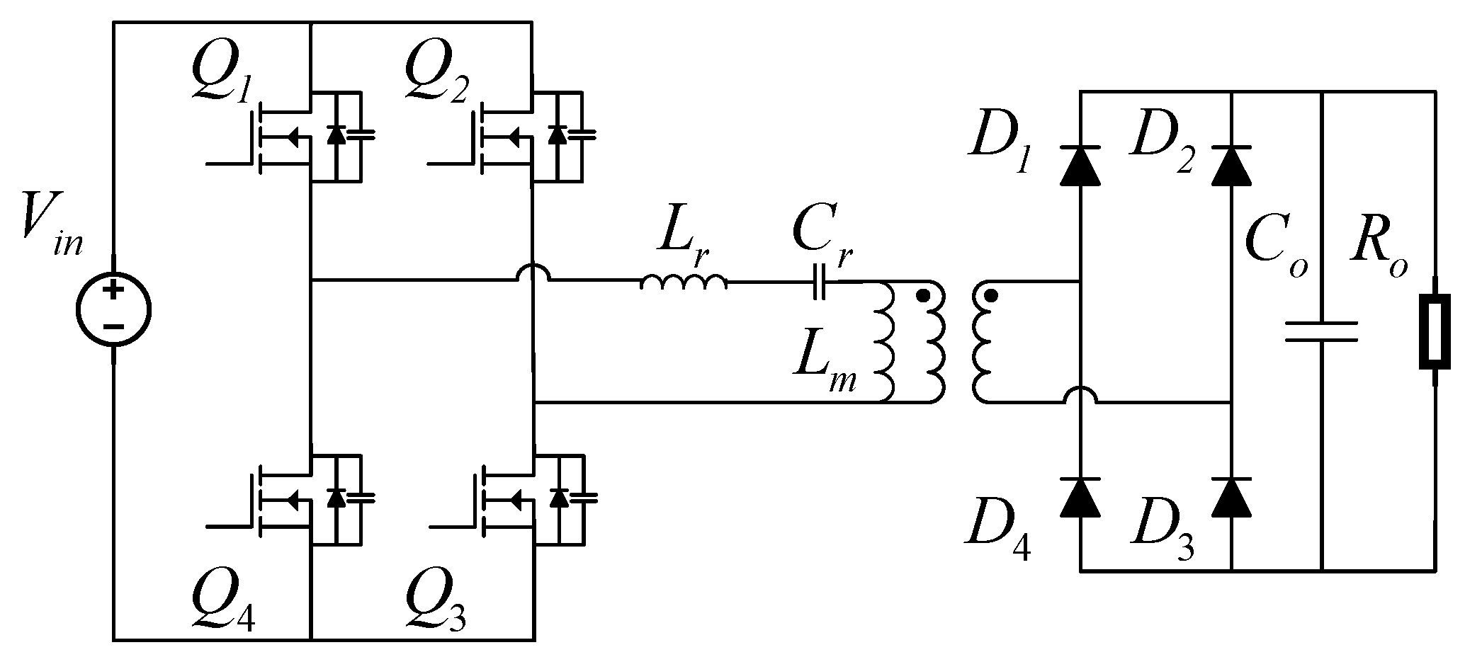
The LLC resonant converter shown in Figure 1 has been widely applied in the field of isolated DC/DC transformation, for example, power adapter, communication power, etc. The LLC resonant converter achieves a first-side MOSFET (Metal-Oxide-Semiconductor Field-Effect Transistor) zero-voltage-switch (ZVS), and a secondary-side rectifier diode zero-current-switch (ZCS), improving the efficiency of the converter [5]. The LLC converter has an excellent efficiency factor in resonant point, but the overall efficiency is lower [6,7,8].
In recent years, with the rise of renewable energy and electric vehicles, LLC resonant converters have been widely applied in high-power fields, and new problems have appeared.
The input and output voltages of the traditional LLC resonant converter are relatively fixed, and the converters work at the rated work point. In photovoltaic applications, the input voltage is not constant whereas the output voltage is constant. In electric vehicle charging applications, the input voltage is constant, the output voltage is not constant, and the load is not constant [9]. These characteristics introduce new requirements for the voltage regulation capability of LLC converters. Previous studies focused on using a staggered parallel system to increase the load gain and capacity of the converter [10]. In [11], additional resonant networks were introduced to increase the boost gain through multiple tap transformers. In [12], the characteristic curve of voltage regulation was changed by adjusting the topological structure.
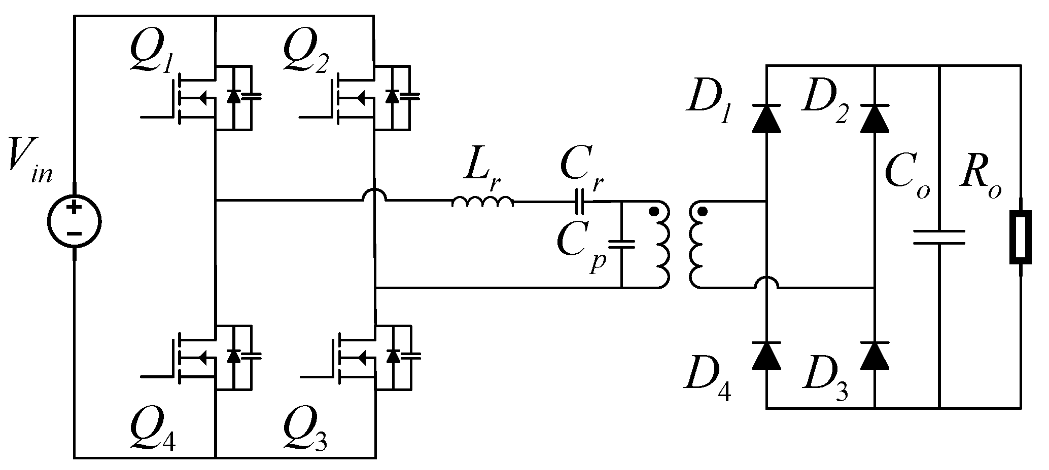
New resonant converters, such as LCC shown in Figure 2 and LCLC converters, have been widely used in industrial applications [13,14,15]. LCC converters gave better load-adjustment characteristics than the LLC converters, but have the disadvantage of significantly changing the switching frequency. A fixed frequency LCC resonant converter is proposed by some scholars, which has the advantages of a simple control circuit, simple design of magnetic components, and so on. However, the fixed frequency LCC resonant converter easily loses the ZVS operation state when the input voltage is increased or the load is decreased [16].
A high-efficiency LLC converter with two split resonant branches is proposed in [8]. It offers two operating modes to obtain a wide range voltage gain. A half-bridge (HB) LLC converter with a single control scheme using one additional switch and small-sized magnetizing LCC was proposed in [17]. The resonant capacitance was changed by turning on or off one additional switch. In [18], a new control method where the effective duty ratio was used not to regulate the output voltage, but to minimize the power loss under light-load conditions for the flyback (FB) LLC resonant converter. In conclusion, the frequency modulation mode of the resonant converter, such as the LLC, causes the converter to change the switching frequency to satisfy the voltage regulation requirement, and the actual operating frequency is often 0.5 to three times of the resonant frequency. The iron core is decided by the minimum operating frequency. Increasing the minimum working frequency is an effective way to reduce the volume of iron core.
The SC (switched-capacitor) structure is widely used to improve the performance of resonant converters. In [19,20], a quasi-switched-capacitor (QSC) resonant converter was proposed to get a higher power density and efficiency for isolated DC/DC conversion. In [21], a quasi-resonant buck converter was proposed to achieve ZVS and an improved voltage gain range.
This paper proposes a constant-frequency LLSC quasi-resonant converter. The resonant capacitor is connected with a set of MOSFET (metal oxide semiconductor field effect transistor) in reverse series in parallel to adjust the equivalent capacitance in the resonant cavity and adjust the reactance. The converter adjusts the output voltage by changing the drive delay. The primary-side-MOSFFETs work in the ZVS condition. The additional MOSFETs have an excellent loss factor. Compared with the LLC converter, the proposed converter has a better overall efficiency.
This paper is divided into the following sections. Section 2 provides an improved topology to describe the commutation process. Section 3 describes the voltage gain factor. Section 4 describes the switching condition. In Section 5, comparisons are made on the efficiency factor, loss, and volume of iron core. Section 6 makes conclusions.
2. The Proposed LLSC Converter and Its Operational Principle
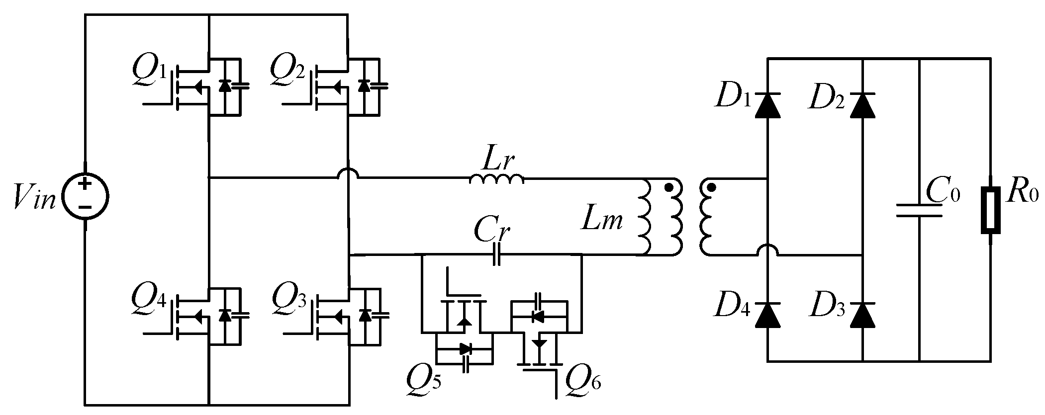
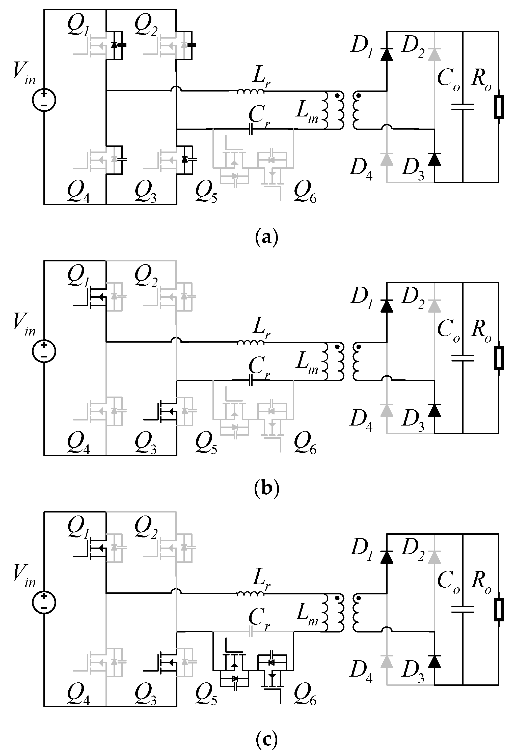
In this chapter, the structure of the LLSC is proposed and is shown in Figure 3. Cr is connected in parallel with a group of inverse series MOSFET to form an adjustable capacitance. The bypass branch’s forward conduction condition is the conduction of the forward MOSFET and body diode of the reverse bypass MOSFET.
The full-bridge have a set of complementary drivers with dead zones, which is the same as an LLC converter. Different from LLC converters, the operating frequency of the LLSC converter’s Q1–Q4 is constant. The additional MOSFET’s Q5 and Q6 have another set of complementary drivers, whose operating frequency is the same as Q1–Q4’s.
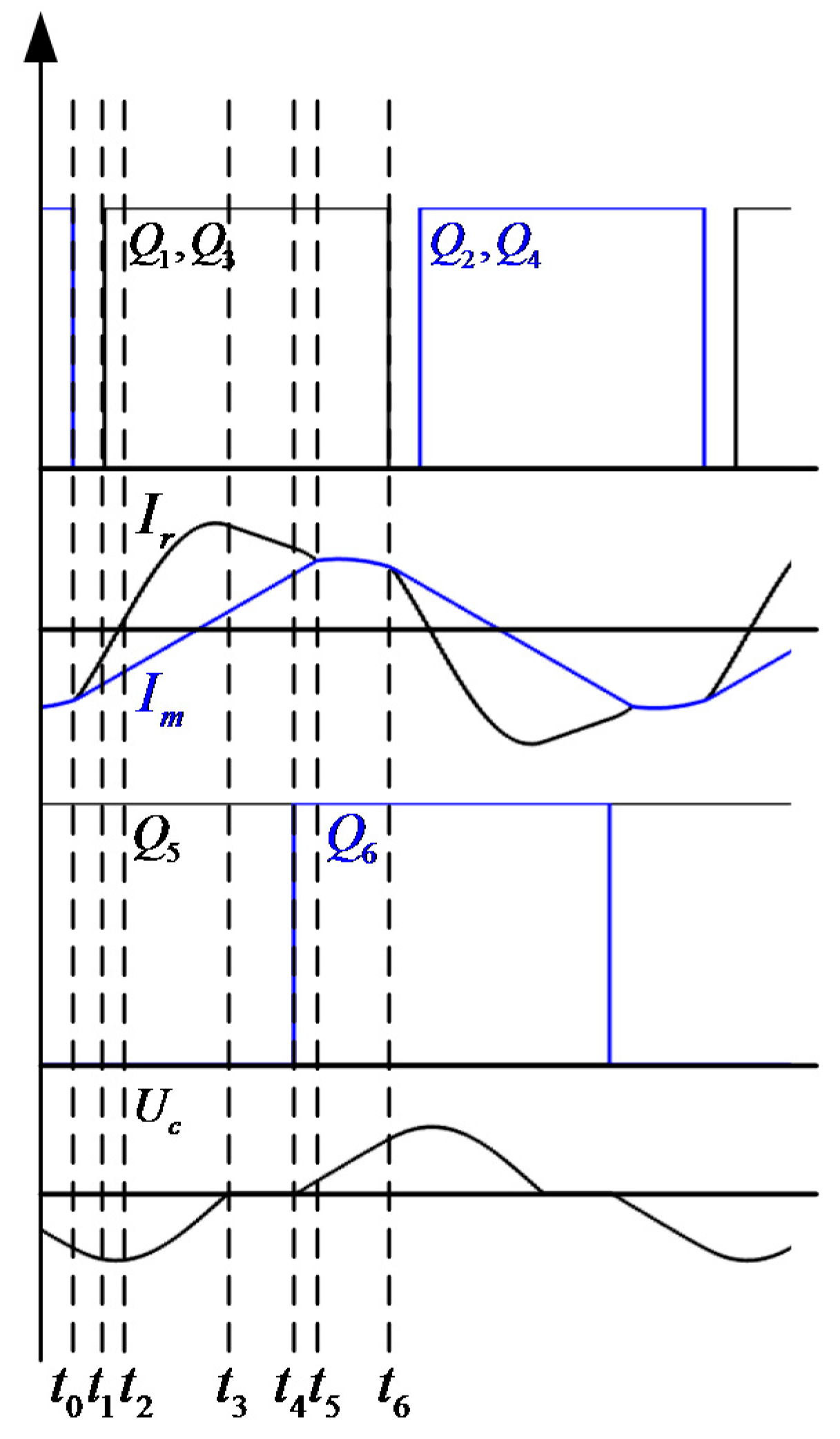
Because the operating frequency of the LLSC converter does not change, the working range is divided by the way of the boost mode and the buck mode. Figure 4 shows the key waveforms of the LLSC converter. Figure 5 shows the equivalent circuits for each switching state.
Boost mode: State 1 [t0–t1] (Figure 5a): Before t0, switches Q2 and Q4 are turned on. At t0, Q2 and Q4 are turned off. The forward bypass MOSFET Q5 keeps a high driver. Because the resonant capacitor’s voltage is negative, the body diode of the reverse bypass MOSFET cannot conduct, so the bypass branch is not conducted, the resonant capacitor is involved in the resonance, and the capacitor voltage is increasing. The current reversely flows through the body diode and continuously decreases. When the secondary diodes, D1 and D3, are conducted, the field inductor, , is clamped by the output voltage, and the field current is linearly reduced. During this period, the ZVS is achieved.
State 2 [t1–t2] (Figure 5b): Q1 and Q3 are turned on, and the voltage in the resonant cavity becomes positive. The resonant current decreases. At , the resonant current is zero and the resonant capacitor’s voltage reaches its peak.
State 3 [t2–t3] (Figure 5b]: The capacitor’s voltage decreases with the increase of resonant current. At t3, the capacitor’s voltage is zero. The body diode of the reverse bypass MOSFET conduct. The resonant capacitor is bypassed.
State 4 [t3–t4] (Figure 5c]: Because of the exit of the resonant capacitor, the resonant current decreases in a line. At t4, the forward bypass MOSFET Q5 is given a low driver and is turned off. The resonant capacitor participates in the resonance. The reverse bypass MOSFET is given a high driver. Because the resonant capacitor’s voltage is positive, the body diode of the forward bypass MOSFET cannot conduct.
State 5 [t4–t5] (Figure 5b]: The resonant current decreases. At t5, the resonant current and field current are equal. The circuit enters the intermittent state. The field inductor, Lm, is no longer clamped by the output voltage, and participates in the resonance.
State 6 [t5–t6] (Figure 5d]: The circuit works in the intermittent state. At , Q1 and Q3 are turned off. The circuit enters the dead time. The parasitic capacitors of the MOSFETs perform the energy conversion under the field current, which is a preparation for the ZVS.
Because of the symmetry of the full bridge converter, the lower half cycle is identical to the upper half.
Buck mode: The difference between the boost and buck modes is the driver delay of Q5 and Q6. The length of the delay is related to the load and the resonance parameters. The commutation process is similar to the boost mode, which is not mentioned in this article.
3. Voltage Gain Characteristic of the LLSC Converter
In Section 2, the operational principle of the LLSC converter is described. In this section, the voltage gain and soft-switching of the LLSC converter are discussed.
3.1. The Relationship between Equivalent Capacitance and Driver Delay
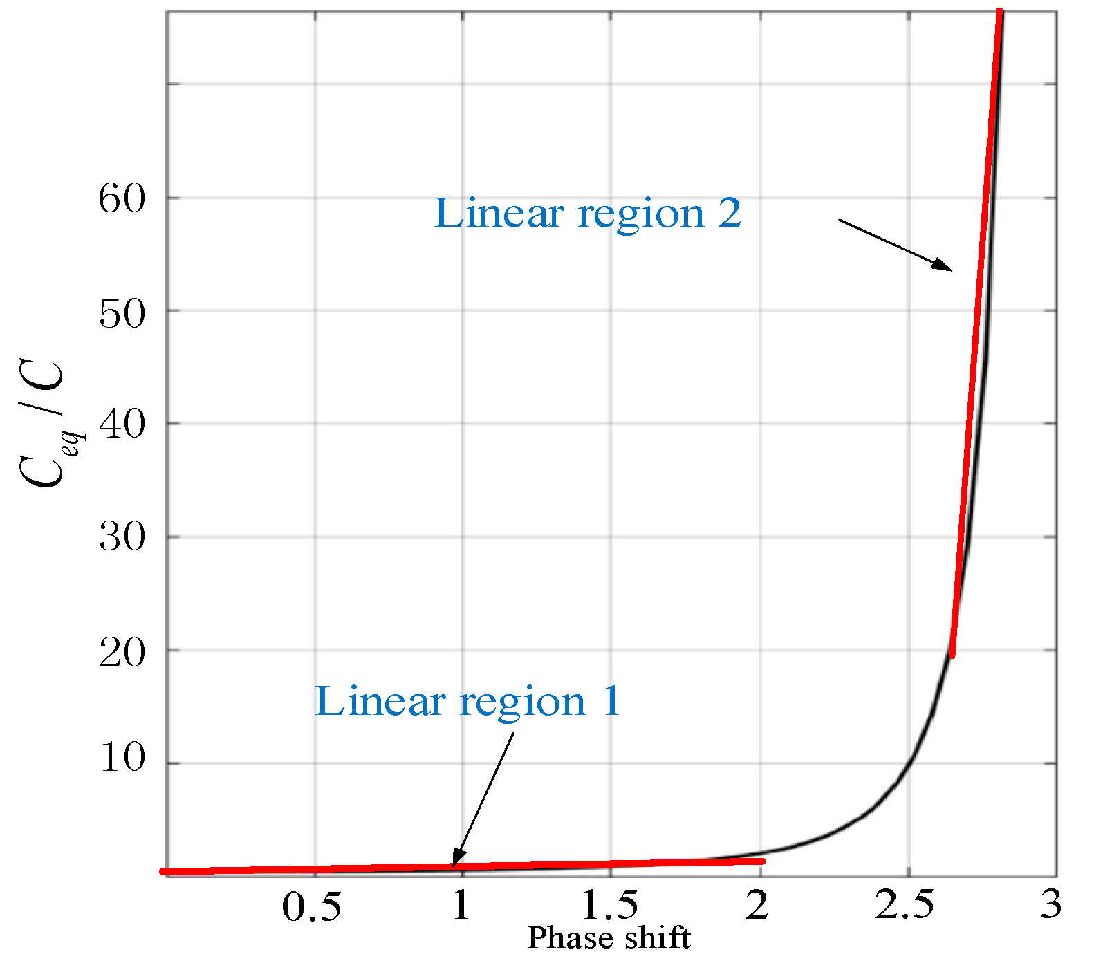
The SC structure was first proposed in [22]. The principle of the work is not described in detail in this article. The working state of the SCC can be divided into two categories: Full wave and half wave. Because the use of the SC is used as a resonant capacitor, the full wave switch-control-capacitor (SCC) structure is adopted in this paper.
The equivalent capacitance of a full wave SCC are derived as follows and is shown in Figure 6:
where Ce is the equivalent capacitance and C is the basic capacitance.
There are two linear regions that can be chosen. The first one is gentle, but has a small-range. The second one is steep, but has a large range. It is necessary to select the appropriate linear region by combining the voltage gain model.
3.2. The Relationship between the Voltage Gain and Equivalent Capacitance
After we simplify the SCC structure, the LLSC converter has the same structure as the LLC converter. Therefore, the fundamental harmonic analysis (FHA) model can be used to describe the voltage gain of the LLSC converter.
The LLC’s gain of the FHA model can be expressed by the following equation:
where , , .
The FHA model describes the relationship between the voltage gain and operating frequency. The LLSC converter is a constant frequency converter, and the FHA should describe the relationship between the voltage and the equivalent capacitance. Therefore, some changes should be made for the FHA model.
where .
Equation (3) has two free degree, x and Q, which contain Cr. With the increase of Cr, x decreases. Therefore, the gain curve of the LLSC converter has the same trend as the LLC converter. The voltages are shown in Figure 7.
From Figure 7, it is clear that a small range of the equivalent capacitance is needed to achieve the remainder of the voltage adjustment. Therefore, the linear region 1 is selected for the LLSC converter.
4. The Soft Switching Character of the LLSC Converter
For the LLC converter, the turn-off current and operating frequency are the influential factor of the loss. The ZVS condition must be achieved to achieve a high efficiency. The LLSC converter works at a constant operating frequency that has some different characteristics to the LLC converter.
4.1. The ZVS Character of the LLSC Converter
There are six MOSFETs, which are divided in two sets (Q1–Q4) (Q5, Q6). The first set’s work condition is similar to the LLC converter. To achieve the ZVS, enough positive resonant current should be satisfied. From the impedance’s angle, the resonant cavity must be inductive. In the design of the LLC converter, the minimum operating frequency is set to ensure that the circuit has enough forward resonant current to achieve the ZVS. In the FHA model, the ZVS problem is described in the following form:
There are two resonant points in the FHA model, which are named as the first resonance point and the second resonance point. The first means that only Lr and Cr participate in the resonance. The second means that Lr, Cr, and Lm participate in the resonance. At the second resonance, the resonant cavity’s impedance is zero. The minimum operating frequency must be higher than the second resonance point. However, in fact, the minimum operating frequency can only guarantee the direction of the resonant current, which can not guarantee enough resonant current. In the case of operation, the possibility of ZVS failure exists in the LLC converter.
For the LLSC converter, the ZVS problem is decided by the means of the basic capacitance, C. The LLSC changes the resonant cavity’s equivalent impedance through the bypassing of the resonant capacitor. When the bypass branch does not work, the capacitive impedance is the largest. This means the basic capacitance decides the ZVS condition. If a suitable capacitance value is selected, the converter keeps the ZVS state in the full range of work. This is the first advantage of the LLSC converter compared with the LLC converter.
4.2. The Turn-Off Loss of the LLSC Converter
The shut down current and operating frequency are two main factors that affect shut down loss.
In the boost mode, the turn-off loss occupies most of the loss. Reducing the shut down current is an effective means to reduce the turn-off loss. Compared with the LLC converter, the LLSC converter can offer a smaller shut down current.
The resonant current can be divided into three parts. The first part represents the stage in which the capacitance is involved in the resonance. This part can be described in the following equation:
where .
Compared with the LLC converter, the LLSC converter has a smaller resonant capacitance, which can offer a faster change rate of the resonant current. In the first part, the LLSC converter can transfer more power.
In the second part, only the resonance inductor participates in the resonance and the resonant current tends to be gentle.
In the third part, the resonance inductor and excitation inductor participate in the resonance.
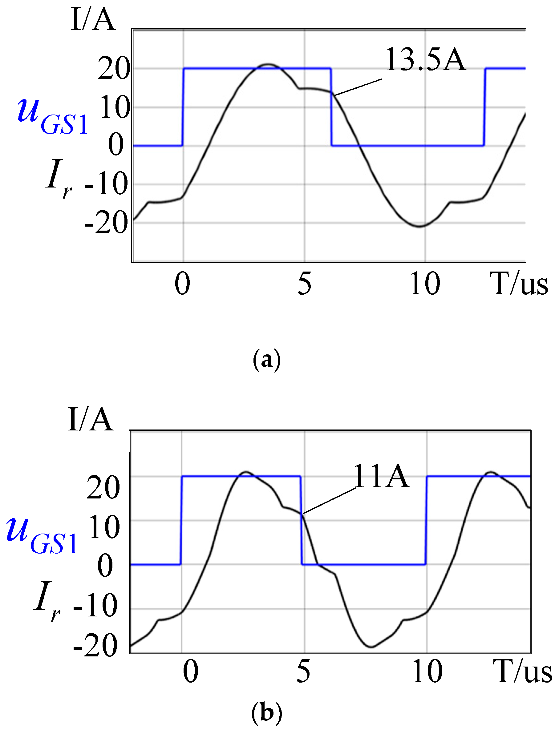
From Figure 8, the LLSC converter’s turn-off current is smaller than that of the LLC converter’s.
In the buck mode, the LLSC converter works at a lower operating frequency that can effectively reduce turn-off loss.
4.3. The Loss Character of the LLSC Converter’s Additional MOSFETs
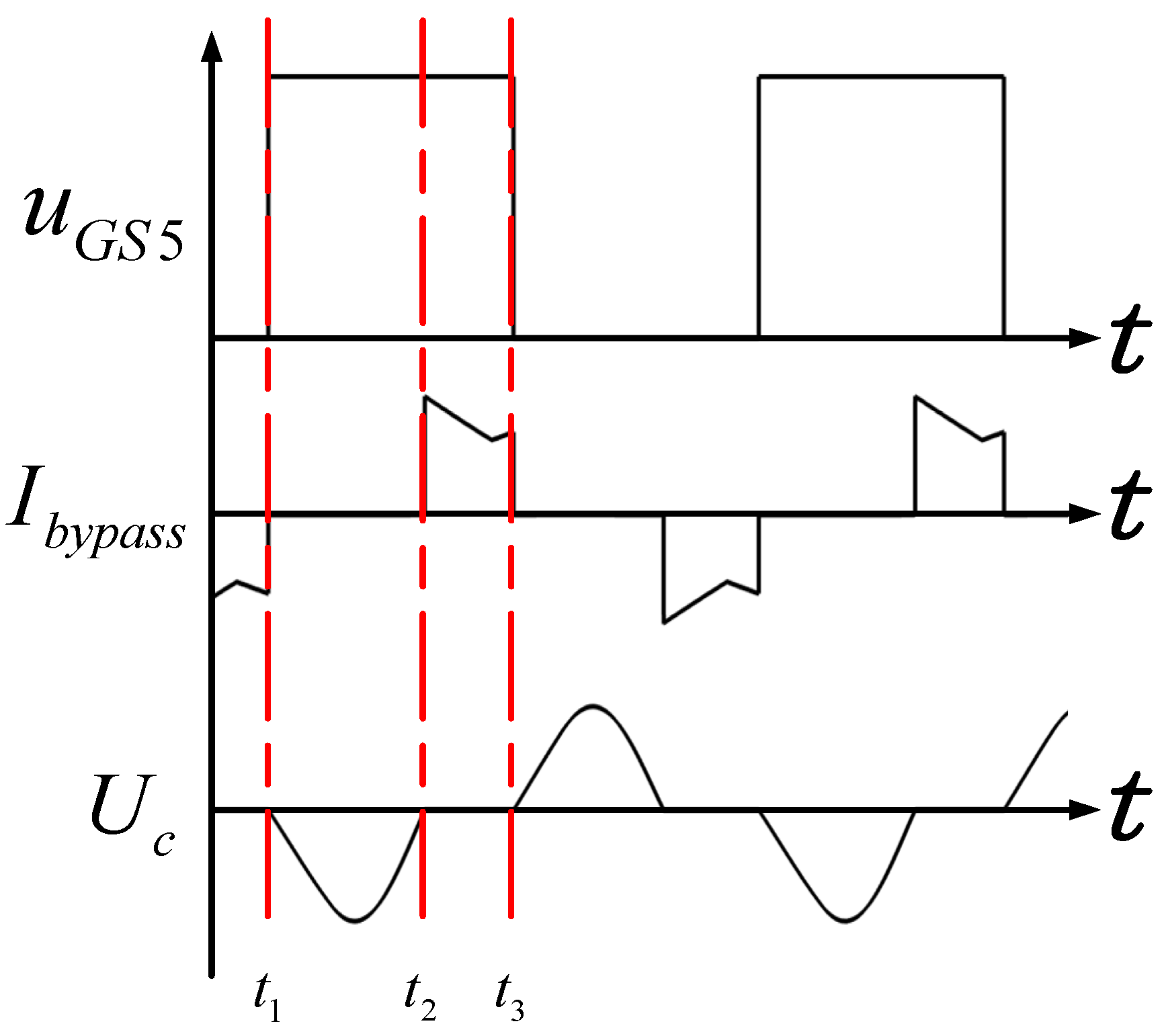
The forward bypass branch consists of the forward MOSFET and the body diode of the reverse bypass MOSFET. Therefore, the forward conduction conditions are that the forward MOSFET has a high driver, the resonant cannot have a negative voltage, and the resonant current must be positive. The waves are shown in Figure 9.
At t1 point, the forward MOSFET has a high driver. The forward bypass branch cannot conduct because the resonant current is negative. At t2 point, the resonant current is positive and the resonant capacitor’s voltage decreases to zero. The bypass branch conducts. At t3 point, the forward MOSFET has a low driver and turn-off.
This mode of work leads to a small switching loss. The conduction loss is the main factor of additional MOSFETs.
5. The Comparison between the LLSC Converter and LLC Converter
A LLSC converter prototype was built to verify the impedance voltage regulation method. The final parameters of the LLSC converter and LLC converter are listed in Table 1. To verify the voltage gain curve trend of the LLSC converter, a small value capacitance was selected.
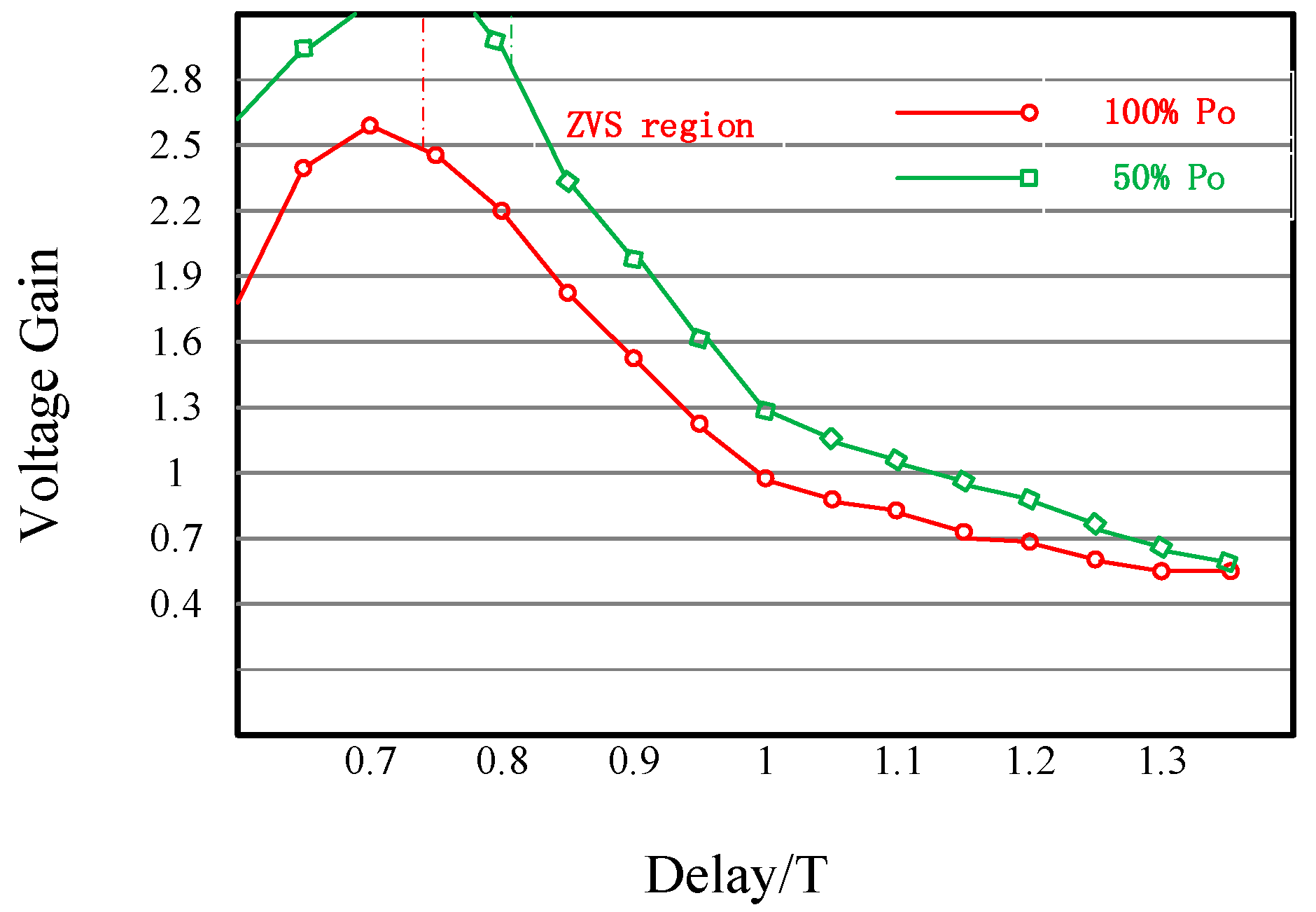
The output voltage was changed by adjusting the driver delay of and . In the experiment, the driver delay increases 5% of the period per time. Figure 10 shows the relationship between the voltage gain and drive delay. The output voltage first increases and then decreases with the increase in capacitance, which is consistent with the analysis in Section 3.
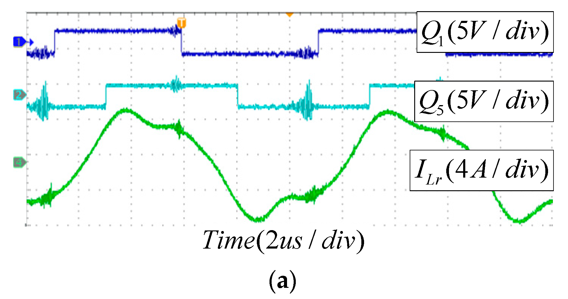
Figure 11 shows the curves in the steady state. The first curve is the driver of Q1, and the second curve is the driver of Q5. The third curve is ILr.
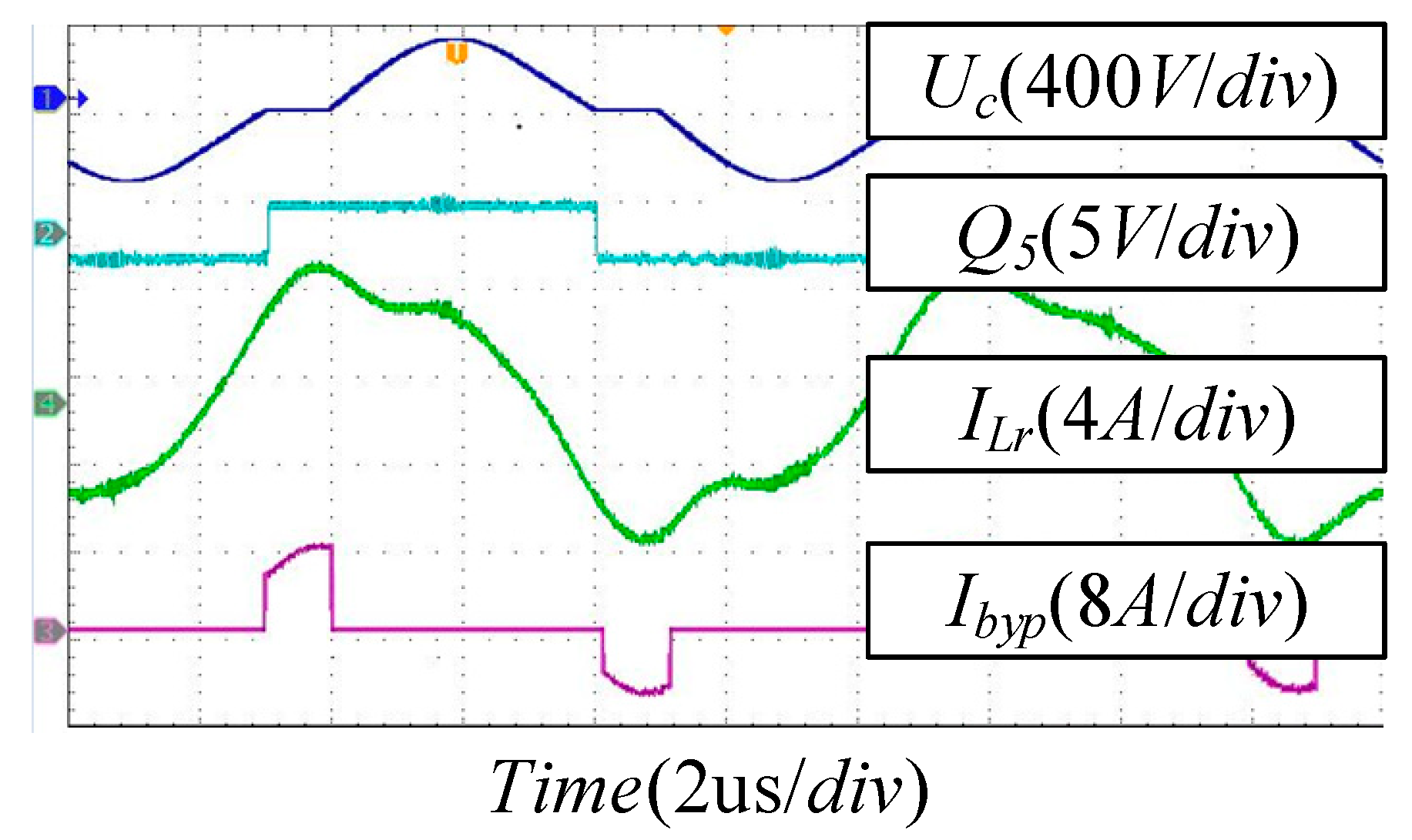
Figure 12 shows the curves in the switching diagram. The first curve is the voltage of the resonant capacitor, and the second curve is the driver of Q5. The third curve is ILr, and the fourth curve is the current of the bypass branch.
To better demonstrate the advantage of the constant frequency converter in the design of magnetic original parts, a comparison of transformer and converter loss were made.
The magnetic core geometric constant method () was used to design a transformer.
The apparent power of the iron core is the sum of the primary side and the secondary side power:
can be described as the following equation:
where , .
can be described as the following equation:
where means the adjustment rate.
According to , the suitable iron core was chosen. The iron loss can be expressed by the following equation:
The following equation is used to estimate the wire turns, which are related to the copper loss:
and come from the parameters of the iron core.
From Table 2, it is clear that the LLSC converter uses a smaller volume, lighter weight, and fewer wire turns transformer, which means a smaller loss.
Finally, the loss parameters and efficiency are compared.
Both converters can achieve the ZVS, therefore, the turn-off is a main factor of the switching loss.
The turn-off loss can be estimated through the following equation:
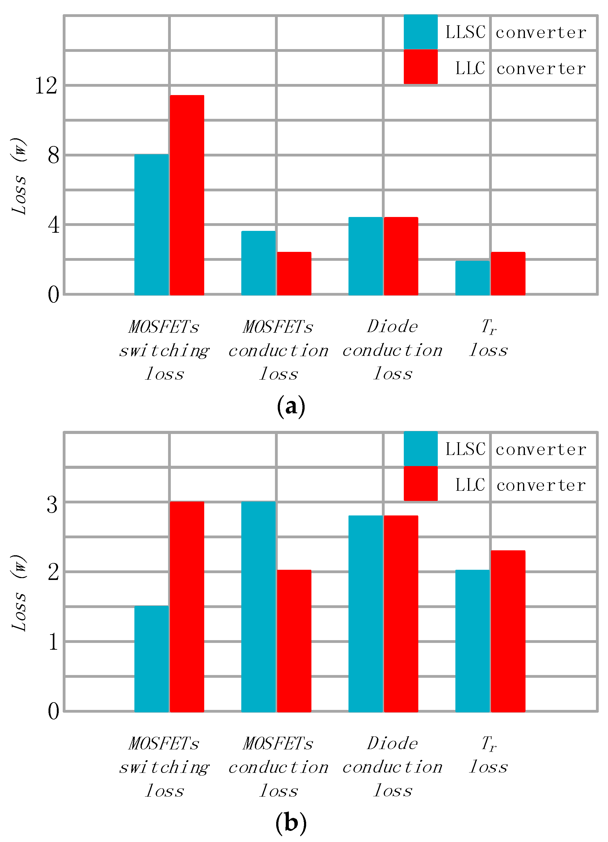
From Figure 13, it is clear that the LLSC converter performs well in terms of switching losses. Due to the larger resistance (0.3 ohm) of MOSFET in the experiment, the conduction accounts for the maximum. The LLSC converter is more efficient with the MOSFET (40 mohm).
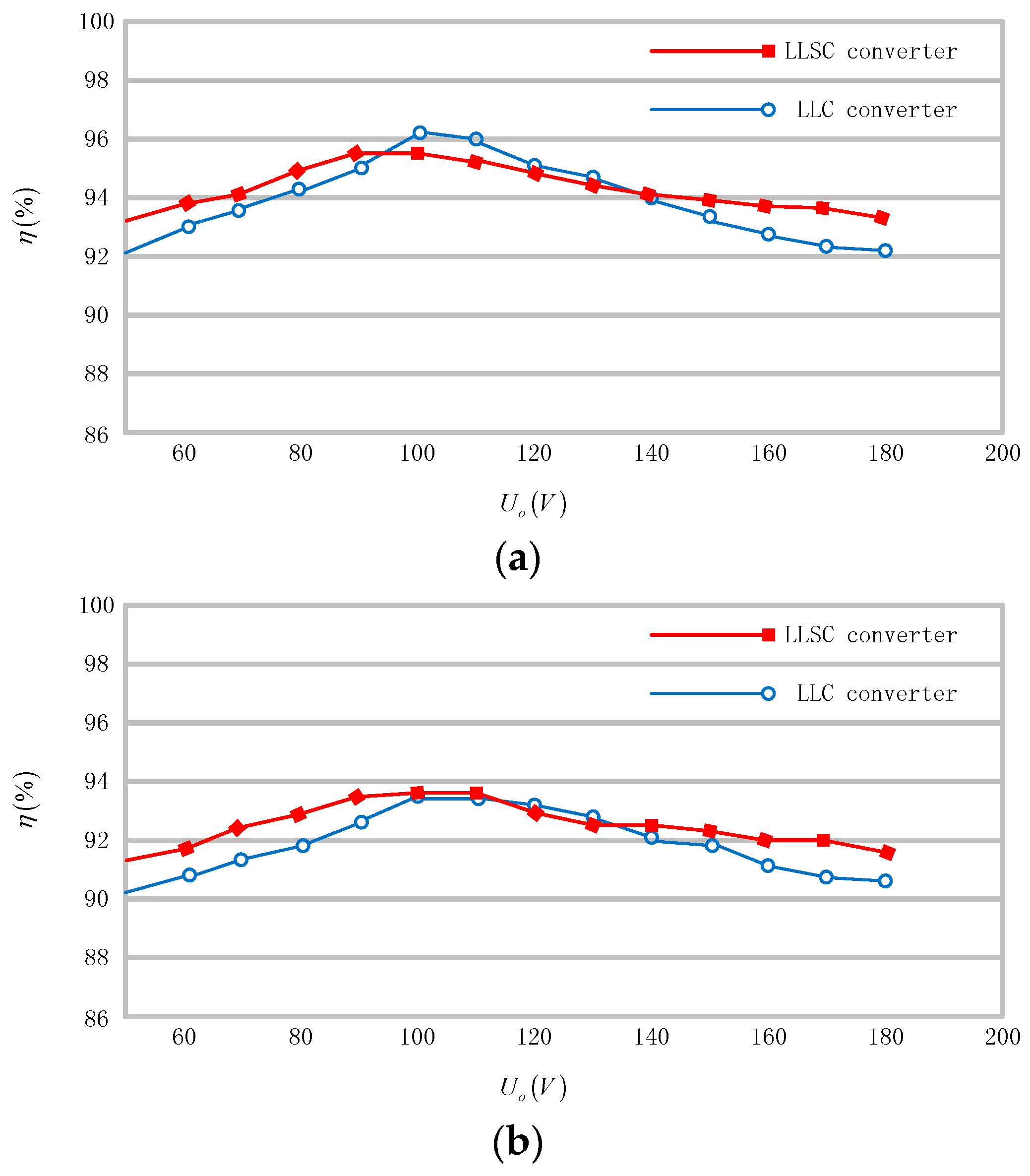
Figure 14 is a comparison of the efficiency between the LLSC converter and the LLC converter. In the buck mode, the LLSC converter has a significant advantage. The LLSC converter has a gentle efficiency curve, which means the LLSC converter is suitable for large range voltage regulation applications.
6. Conclusions
In this paper, a new LLSC quasi-resonant converter was proposed, which achieved impedance voltage regulation at a constant frequency. The proposed converter has a better soft switching factor and higher efficiency. The proposed converter has the following features compared with a traditional LLC converter:
- (1)
- The proposed converter works at a constant frequency, and the volume of the iron core can be reduced by 30%. The number of winding’s turns, winding loss, and iron loss can be reduced;
- (2)
- The output filter capacitance value can be reduced;
- (3)
- The ZVS condition of the MOSFET of the primary side can be ensured using reasonable resonance parameters;
- (4)
- The turn-off loss of the primary side MOSFETs can be reduced by 30% to 50%;
- (5)
- The overall efficiency is improved in wide output-voltage applications; and
- (6)
- A new reactance voltage regulation method is proposed.
The validity of the LLSC converter has been confirmed using a 250 W experimental prototype. The experiment results show that the LLSC converter has the above features. Worth watching, with the application of low on-resistance devices, such as SiC and GaN, the proposed converter achieves a higher efficiency.
Author Contributions
T.Z. designed and performed the experiment. J.W. and Y.J. carried out the study and collected important background information. Y.L. carried out data acquisition and manuscript editing. All authors read and approved the final manuscript.
Conflicts of Interest
The authors declare no conflict of interest.
Nomenclature
| Ce | Equivalent capacitance |
| C | Basic capacitance |
| α | phase shift |
| G | Voltage gain |
| fr | Resonant frequency |
| fs | Switching frequency |
| k | Inductance ratio |
| Q | Quality factor |
| Lr | Resonant inductance |
| Cr | Resonant capacitance |
| Pt | Apparent power |
| Ptp | Apparent power of primary side |
| Pts | Apparent power of secondary side |
| Co | The output capacitance of MOSFET |
| Im | The turn-off current of MOSFET |
| tf | The turn-off time of MOSFET |
References
- Iqbal, S. Double LLC resonant tanks based DC-DC converter with integrated dual transformers for PV power systems. In Proceedings of the 2016 IEEE Power and Energy Conference at Illinois, Urbana, IL, USA, 19–20 February 2016; pp. 1–6. [Google Scholar]
- Buccella, C.; Cecati, C.; Latafat, H.; Razi, K. A grid-connected PV system with LLC resonant DC-DC converter. In Proceedings of the International Conference on Clean Electrical Power, Alghero, Italy, 11–13 June 2013; pp. 777–782. [Google Scholar]
- Chen, J.; Sha, D.; Liao, X. Decentralized control strategy for input-series-output-parallel modular LLC resonant DC/DC converters. In Proceedings of the IEEE Future Energy Electronics Conference, Taipei, Taiwan, 1–4 November 2015; pp. 1–5. [Google Scholar]
- Liang, Z.; Guo, R.; Li, J.; Huang, A.Q. A High-Efficiency PV Module-Integrated DC/DC Converter for PV Energy Harvest in FREEDM Systems. IEEE Trans. Power Electron. 2011, 26, 897–909. [Google Scholar] [CrossRef]
- Narimani, M.; Moschopoulos, G. An Investigation on the Novel Use of High-Power Three-Level Converter Topologies to Improve Light-Load Efficiency in Low Power DC/DC Full-Bridge Converters. IEEE Trans. Ind. Electron. 2014, 61, 5690–5692. [Google Scholar] [CrossRef]
- Musavi, F.; Craciun, M.; Gautam, D.S.; Eberle, W.; Dunford, W.G. An LLC Resonant DC–DC Converter for Wide Output Voltage Range Battery Charging Applications. IEEE Trans. Power Electron. 2013, 28, 5437–5445. [Google Scholar] [CrossRef]
- Shen, Y.; Zhao, W.; Chen, Z.; Cai, C. Full-bridge LLC Resonant Converter with Series-parallel Connected Transformers for Electric Vehicle On-board Charger. IEEE Access 2018, 6, 13490–13500. [Google Scholar] [CrossRef]
- Sun, W.; Xing, Y.; Wu, H.; Ding, J. Modified High-efficiency LLC Converters with Two Split Resonant Branches for Wide Input-Voltage Range Applications. IEEE Trans. Power Electron. 2017, 33, 7867–7879. [Google Scholar] [CrossRef]
- Hermann, R.; Bernet, S.; Yongsug, S.; Steimer, P.K. Parallel connection of integrated gate commutated thyristors (IGCTs) and diodes. IEEE Trans. Power Electron. 2009, 24, 2159–2170. [Google Scholar] [CrossRef]
- Rabkowski, J.; Peftitsis, D.; Nee, H.P. Parallel-operation of discrete SiCBJTs in a 6-kW/250-kHzDC/DC boost converter. IEEE Trans. Power Electron. 2014, 29, 2482–2491. [Google Scholar] [CrossRef]
- Kim, D.K.; Moon, S.C.; Yeon, C.O.; Moon, G.-W. High-Efficiency LLC Resonant Converter with High Voltage Gain Using an Auxiliary LC Resonant Circuit. IEEE Trans. Power Electron. 2016, 31, 6901–6909. [Google Scholar] [CrossRef]
- Kim, C.E.; Baek, J.I.; Lee, J. High-Efficiency Single-Stage LLC Resonant Converter for Wide-Input-Voltage Range. IEEE Trans. Power Electron. 2014, 33, 7832–7840. [Google Scholar] [CrossRef]
- Soeiro, T.B.; Muhlethaler, J.; Linner, J.; Ranstad, P.; Kolar, J.W. Automated design of a high-power high-frequency LCC resonant converter for electrostatic precipitators. IEEE Trans. Ind. Electron. 2013, 60, 4805–4819. [Google Scholar] [CrossRef]
- Li, Z.; Park, C.-Y.; Kwon, J.-M.; Kwon, B.-H. High-powerfactor single-stage LCC resonant inverter for liquid crystal display backlight. IEEE Trans. Ind. Electron. 2011, 58, 1008–1015. [Google Scholar] [CrossRef]
- Tsai, M.C. Analysis and implementation of a full-bridge constantfrequency LCC-type parallel resonant converter. Proc. Inst. Elect. Eng. Electr. Power Appl. 1994, 141, 121–128. [Google Scholar] [CrossRef]
- Czarkowski, D.; Kazimierczuk, M.K. Phase-controlled series-parallel resonant converter. IEEE Trans. Power Electron. 1993, 8, 309–319. [Google Scholar] [CrossRef] [Green Version]
- Lee, J.B.; Kim, J.K.; Baek, J.I.; Moon, G.-W. Resonant Capacitor on/off Control of Half-Bridge LLC Converter for High-Efficiency Server Power Supply. IEEE Trans. Ind. Electron. 2016, 63, 5410–5415. [Google Scholar] [CrossRef]
- Kim, J.H.; Kim, C.E.; Kim, J.K.; Li, J.-B.; Moon, G.-W. Analysis on Load-Adaptive Phase-Shift Control for High Efficiency Full-Bridge LLC Resonant Converter under Light-Load Conditions. IEEE Trans. Power Electron. 2016, 31, 4942–4955. [Google Scholar]
- Zhang, X.; Yao, C.; Wang, J. A Quasi-Switched-Capacitor Resonant Converter. IEEE Trans. Power Electron. 2016, 31, 7849–7856. [Google Scholar] [CrossRef]
- Zhang, X.; Yao, C.; Guo, F.; Wang, J. Optimal operation and burst-mode control for improving the efficiency of the quasi-switched-capacitor resonant converter. In Proceedings of the IEEE Energy Conversion Congress and Exposition, Pittsburgh, PA, USA, 14–18 September 2014; pp. 5444–5450. [Google Scholar]
- Wang, J.; Zhang, F.; Xie, J.; Liu, S. Analysis and design of high efficiency Quasi-Resonant Buck converter. In Proceedings of the IEEE Power Electronics and Application Conference and Exposition, Shanghai, China, 5–8 November 2014; pp. 1486–1489. [Google Scholar]
- Gu, W.J.; Harada, K. A new method to regulate resonant converters. IEEE Trans. Power Electron. 1988, 3, 430–439. [Google Scholar]
Figure 1.
Conventional isolated LLC resonant converter.

Figure 2.
Conventional isolated LCC resonant converter.

Figure 3.
A novel LSCC converter.

Figure 4.
Commutation process of the LLSC converter in the boost mode.

Figure 5.
Conduction circuit of the LLSC converter in the boost mode. (a) Stage 1; (b) Stages 2, 3 and 5; (c) stage 4; and (d) Stage 6.
Figure 5.
Conduction circuit of the LLSC converter in the boost mode. (a) Stage 1; (b) Stages 2, 3 and 5; (c) stage 4; and (d) Stage 6.


Figure 6.
Equivalent capacitance of the full-wave SCC versus phase shift.

Figure 7.
Voltage gain curves of the impedance voltage regulation by the FHA model.

Figure 8.
Current trend comparation of the LLSC converter and LLC converter at the same load. (a) LLC converter (80 kHz) and (b) LLSC (100 kHz).
Figure 8.
Current trend comparation of the LLSC converter and LLC converter at the same load. (a) LLC converter (80 kHz) and (b) LLSC (100 kHz).

Figure 9.
Soft switching diagram of the LLSC converter’s additional MOSFETs.

Figure 10.
Relation between the voltage gain and drive delay.

Figure 11.
Relationship between the current and the driver in the steady state. (a) Output voltage 150 V; (b) output voltage 130 V; (c) output voltage 90 V; and (d) output voltage 70 V. The output voltage decreases with the increase in the drive delay.
Figure 11.
Relationship between the current and the driver in the steady state. (a) Output voltage 150 V; (b) output voltage 130 V; (c) output voltage 90 V; and (d) output voltage 70 V. The output voltage decreases with the increase in the drive delay.


Figure 12.
Key waves in switching diagram.

Figure 13.
Loss comparison between the LLSC converter and LLC converter. (a) Output voltage 250 V and (b) output voltage 50 V.
Figure 13.
Loss comparison between the LLSC converter and LLC converter. (a) Output voltage 250 V and (b) output voltage 50 V.

Figure 14.
Efficiency comparison between the LLSC converter and LLC converter. (a) 100% load and (b) 50% load.
Figure 14.
Efficiency comparison between the LLSC converter and LLC converter. (a) 100% load and (b) 50% load.


Table 1.
Experiment parameters.
| Parameters | LLSC | LLC |
|---|---|---|
| Input voltage | 200 V | 200 V |
| Output voltage | 50–250 V | 50–250 V |
| Resonant inductance | 50 uH | 50 uH |
| Resonant capacitor | 20 nF | 50 uF |
| Magnetic inductance | 100 uH | 100 uH |
| Transformer ratio | 2:1 | 2:1 |
| Operating Frequency | 100 kHz | 65–300 kHz |
| Power rating | 250 W | 250 W |
Table 2.
Magnetic substance parameters.
| Parameters | LLSC | LLC |
|---|---|---|
| Power rating | 250 W | 250 W |
| Minimum operating frequency, f | 100 kHz | 65 kHz |
| Kg of transformer | 0.0699 cm5 | 0.1656 cm5 |
| Iron core model | PQ26/25 | PQ32/30 |
| Iron core weight | 36 g | 55 g |
| Primary side’s wire turns | 76 | 86 |
| Secondary side’s wire turns | 38 | 43 |
| Iron loss | 0.11 W | 0.17 W |
| Copper loss | 1.88 W | 2.32 W |
| Total loss | 2 W | 2.5 W |
© 2018 by the authors. Licensee MDPI, Basel, Switzerland. This article is an open access article distributed under the terms and conditions of the Creative Commons Attribution (CC BY) license (http://creativecommons.org/licenses/by/4.0/).
Share and Cite
MDPI and ACS Style
Zhu, T.; Wang, J.; Ji, Y.; Liu, Y. A Novel High Efficiency Quasi-Resonant Converter. Energies 2018, 11, 1961. https://doi.org/10.3390/en11081961
AMA Style
Zhu T, Wang J, Ji Y, Liu Y. A Novel High Efficiency Quasi-Resonant Converter. Energies. 2018; 11(8):1961. https://doi.org/10.3390/en11081961
Chicago/Turabian StyleZhu, Tianyu, Jianze Wang, Yanchao Ji, and Yiqi Liu. 2018. "A Novel High Efficiency Quasi-Resonant Converter" Energies 11, no. 8: 1961. https://doi.org/10.3390/en11081961
Note that from the first issue of 2016, this journal uses article numbers instead of page numbers. See further details here.