
Abstract
We report bias enhanced nucleation and growth of boron-rich deposits through systematic study of the effect of a negative direct current substrate bias during microwave plasma chemical vapor deposition. The current flowing through a silicon substrate with an applied bias of −250 V was investigated for a feedgas containing fixed hydrogen (H2) flow rate but with varying argon (Ar) flow rates for 1330, 2670, and 4000 Pa chamber pressure. For 1330 and 2670 Pa, the bias current goes through a maximum with increasing Ar flow rate. This maximum current also corresponds to a peak in substrate temperature. However, at 4000 Pa, no maximum in bias current or substrate temperature is observed for the range of argon flow rates tested. Using these results, substrate bias pre-treatment experiments were performed at 1330 Pa in an Ar/H2 plasma, yielding the maximum bias current. Nucleation density of boron deposits were measured after subsequent exposure to B2H6 in H2 plasma and found to be a factor of 200 times higher than when no bias and no Ar was used. Experiments were repeated at 2670 and 4000 Pa (fixed bias voltage and Ar flow rate) in order to test the effect of chamber pressure on the nucleation density. Compared to 4000 Pa, we find nearly 7 times higher boron nucleation densities for both 1330 and 2670 Pa when the substrate was negatively biased in the Ar/H2 plasma. Results are explained by incorporating measurements of plasma optical emission and by use of heterogeneous nucleation theory. The optimal conditions at 1330 Pa for nucleation were used to grow boron-rich amorphous films with measured hardness as high as 58 GPa, well above the 40 GPa threshold for superhardness.
Export citation and abstract BibTeX RIS
1. Introduction
In chemical vapor deposition (CVD) of films on silicon substrates, diamond slurry is often used to scratch the silicon surface in order to enhance nucleation through formation of high surface energy nucleation sites [1]. Such nucleation sites can decrease the work required for nucleation of a cluster of critical radius in heterogenous nucleation [2]. A DC (direct current) has been used to negatively bias silicon substrates in order enhance nucleation; this method has led to a higher nucleation density when compared to substrates that have been scratched by diamond. This process, known as bias enhanced nucleation (BEN), became popular in CVD growth of diamond after Yugo et al reported its effect on substrates pre-treated in a high methane plasma for several minutes [3]. Applying a negative DC substrate bias creates an electric field, thus directing the motion of ions towards the substrate [4]. Usually, the substrate is the cathode and the CVD chamber is the anode. BEN was first used to nucleate diamond in CVD and it was eventually used to nucleate cubic boron nitride [5].
Today, there is a high interest to study boron-rich materials, because of their potential for high hardness and high temperature oxidation resistance [6]. Several experimental conditions have been used to synthesize boron carbides using different techniques and a variety of boron precursors [7–9]. The most economically feasible methods are carbothermic or magnesiothermic reactions, often used industrially to manufacture boron carbide [10–12]. However, these methods are prone to impurities in the final product. High-pressure high-temperature cells are also used to produce novel boron-rich boron carbide, but they are limited to very small volumes of material [7]. High-pressure high-temperature methods are not easily scalable and can be difficult to control impurities. Instead, CVD has proven to be a scalable technology for synthesizing a wide range of coating materials including boron carbide with large area uniformity [8, 13]. A primary challenge of CVD is to find optimum conditions that are favorable for the growth of the desired phase. In this work, extensive external bias voltage conditions with different gas mixture and flow rates were tested to determine ideal growth conditions for superhard boron-rich material.
The study of BEN of boron-rich materials by CVD is lacking in literature and is therefore the topic of the current work. In MPCVD, a feedgas containing H2 and Ar is commonly used during BEN. The heavy mass of Ar makes it favorable for use in etching as it transfers more energy to a target through change of momentum [14]. Here, Ar will be used to lightly etch the silicon substrate due to ion bombardment. It has been reported that in a glow discharge, electrical current between electrodes varies with the concentration of H2 added to an Ar plasma, such that the current due to ions changes non-linearly with increased concentration of H2 [15]. This work is motivated by a need to analyze how varying Ar and/or H2 concentration in an Ar/H2 plasma can affect the current flow through a substrate due to ion bombardment in MPCVD. Since MPCVD is regularly used for BEN, this work was aimed at finding a maximum current through the silicon substrate due to ion bombardment from an Ar/H2 plasma. For this high current flow, an Ar/H2 plasma was used to pre-treat the silicon substrate prior to nucleation of boron-rich deposits using diborane (B2H6 + H2) in the feed gas.
2. Experimental details
The MPCVD setup is shown in figure 1 (Wavemat Inc. Plymouth, MI, USA). The substrate was heated by direct contact with the plasma. Both the stage and outer resonance cavity jacket were water-cooled. The substrate temperature, Ts, was measured using an optical pyrometer. A quartz bell jar isolated the low-pressure plasma environment from the resonance cavity. N-type (100)-oriented silicon substrates with 525  thickness was placed on the surface of a 0.5' diameter molybdenum screw aligned along the central axis of the bell jar. The substrate was cleaned in acetone, methanol and distilled water. The bias voltage was provided by a Sorensen DCS 600–1.7E power supply. The negative terminal was connected to the molybdenum screw, and the ground was connected on the outer surface of the MPCVD chamber. This allowed the substrate to be negatively biased relative to the walls of the chamber.
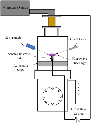
Figure 1. Schematic diagram of the MPCVD chamber showing plasma confined within quartz bell jar.
Download figure:
Standard image High-resolution imageFor all experiments, the microwave power was fixed at 0.6 kW and the H2 carrier gas' flow rate was fixed at 500 standard cubic centimeters per minute (SCCM). The bias voltage applied to the silicon substrate was fixed at − 250 V. Voltage between − 200 V to − 300 V has been regularly used for BEN on silicon substrates by MPCVD [16–18]. While higher or lower bias voltage could have potentially been explored, − 250 V was a safe voltage to nucleate boron-rich materials on silicon by MPCVD. Ar flow rate was varied between 0 and 500 SCCM in order to find a maximum current flowing through the substrate due to variation of Ar. Chamber pressure was controlled by an exhaust throttle valve that regulates the removal of gas from the chamber via a flapper that is positioned to modulate gas flow. Initial experiments were run at 1330 Pa. For each increment in Ar flow rate, the current flowing through the substrate was measured. Measurements of current were repeated at 2670 and 4000 Pa.
After a maximum current was found at 1330 Pa for a given Ar flow rate, the silicon substrate was pre-treated for 30 min in the Ar/H2 plasma. Ar was then turned off and diborane (5% B2H6 in H2, with low ppm levels carbon) was introduced at a flow rate of 2 SCCM to the pure H2 plasma for 15 min in order to nucleate high boron content material on the pre-treated and negatively biased silicon substrate. Residual carbon has been found to appear consistently in the high-boron nucleation [19, 20]. Direct evidence for unintentional and, at the same time, unexpected carbide formation during high-vacuum growth of transition metal nitride thin films has been reported without a carbon source in the feedgas [21]. Possible sources of incorporated carbon during film growth include residual gas impurity as well as outgassing from chamber walls. Stainless steel is the most widely used hardware material for vacuum application. Gases are adsorbed on the surface during operation or air exposure, setting a limit achieving extremely high vacuum, and becoming a source of contamination in high purity processes. It has been found that on the fresh metal surface a few layers of oxides are formed, and on that layer carbon compound contaminants accumulate [22]. Given the high reactivity of boron with carbon, B-C bonds are likely to form during MPCVD film growth, even in a feedgas containing diborane and hydrogen.
The nucleation was then viewed under an optical microscope at 100X magnification. The corresponding image was converted into binary image using Fiji ImageJ [23, 24]. Image contrast was adjusted such that the silicon substrate was set to black and the nuclei set to white. The number of nuclei per unit area was counted using Image-based Tool for Counting Nuclei (ITCN) [25]. This was repeated at 2670 and 4000 Pa in order to test for the effect of pressure on nucleation density.
In order to investigate the effects of DC bias and Ar in the plasma on nucleation density, four experiments were carried out at 1330 Pa (labelled 1–4), at 2670 Pa (labelled 5–8), and at 4000 Pa (labelled 9–12), as summarized in table 1. In experiment 1, 5, and 9, Ar is used in H2 plasma with the negative bias prior to the nucleation step at the respective pressure. The argon ion energy was 250 eV. Experiments 2, 6, and 10 serve as controls (no DC bias) in order to evaluate the effect of DC bias on nucleation density. The argon ion energy was 0 eV. Experiments 3, 7, and 11 serve as controls (no Ar) in order to evaluate the effect of Ar-etching the silicon substrate, leading to increased surface roughness prior to nucleation. Experiments 4, 8, and 12 serve as controls (no Ar or DC bias) in order to evaluate the effect that both Ar and DC bias have on nucleation density.  in table 1 was recorded during nucleation. The highest nucleation density at each pressure occurs when the silicon substrate was exposed to Ar/H2 plasma with a bias voltage. The lowest nucleation density occurs when the silicon substrate was neither exposed to Ar nor to a bias voltage prior to nucleation.
Table 1. Summary of nucleation density results. When a DC bias is used to pre-treat the substrate for 30 min, the bias is also used for BEN for an additional 15 min. The current listed is the measured current during BEN in H2/B2H6 plasma. The nucleation diameter is average of most nucleation diameters and the uncertainty is the standard deviation. The nucleation density is counted after nucleation. Ts is the average substrate temperature during nucleation and the uncertainty is the standard deviation.
| Pressure (Pa) | Label | Ar flow (SCCM) | DC bias (-V) | Ion energy (eV) | Current (A) | Nucleation density ( ) ) | Nucleation diameter 
|
 (°C) (°C) |
|---|---|---|---|---|---|---|---|---|
| 1330 | 1 | 100 | 250 | 250 | 0.022 |

|

|

|
| 2 | 100 | 0 | 0 | 0 |

|

|

| |
| 3 | 0 | 250 | 250 | 0.023 |

|

|

| |
| 4 | 0 | 0 | 0 | 0 |

|

|

| |
| 2670 | 5 | 100 | 250 | 250 | 0.015 |

|

| |
| 6 | 100 | 0 | 0 | 0 |

|

|

| |
| 7 | 0 | 250 | 250 | 0.014 |

|

|

| |
| 8 | 0 | 0 | 0 | 0 |

|

|

| |
| 4000 | 9 | 100 | 250 | 250 | 0 |

|

|

|
| 10 | 100 | 0 | 0 | 0.03 |

|

|

| |
| 11 | 0 | 250 | 250 | 0 |

|

|

| |
| 12 | 0 | 0 | 0 | 0.04 | 5
|

|

|
At 1330 Pa and power 0.6 kW, an additional experiment was performed to grow a continuous film. For the first 45 min, the experiment that lead to highest nucleation density was reproduced. Then for another 5 h and 45 min, 500 SCCM of H2 and 2 SCCM of B2H6 was used at 0.6 kW to grow the boron-rich film without DC bias. Investigation of the excited state plasma species from optical emission spectroscopy (OES) in our MPCVD shows that emission from atomic boron is highest at low chamber pressure [26]. Ample amounts of atomic boron in the plasma may be advantageous under some growth conditions. The film was characterized using glancing angle x-ray diffraction (XRD) and nanoindentation.
The XRD instrumentation was a Panalytical Empyrean x-ray diffractometer (Copper Kα1, λ = 1.54059 Å) (Malvern, Panalytical, Almelo, Netherlands). XRD was acquired using a glancing angle  scan with an angle of incidence of 1°. The diffraction optics included a hybrid monochromator with a 1/8° divergence slit and an 1/16° anti-scattering slit and a parallel plate collimator on the diffracted beam path with a proportional detector. HighScore Plus software (version 4.8) was used to analyze phase structure.
Hardness was measured using an MTS NanoIndenter G200 with a Berkovich diamond tip (nominal radius 50 nm). The calibration of the indenter area function before and after hardness measurements was tested for the fused silica standard (accepted Young's modulus of 72 GPa) to confirm that the tip geometry did not change during the testing of all samples. All indents, including those on silica, were made to a maximum depth of 300 nm. The measured hardness was determined at maximum load. The range of measured silica before/after Young's modulus values was found to be consistent with the accepted value, and therefore the indenter tip area function was determined not to have changed significantly during actual sample testing.
3. Results
At 1330 and 2670 Pa, there was a maximum in current at 100 SCCM and 250 SCCM Ar flow respectively. However, there was no maximum in current found at 4000 Pa for the Ar flow range tested. The experiments were repeated 5 times to test for reproducibility and the average result is displayed in figure 2. The error bars are the standard deviation of the results. Figure 3 shows comparison of four binary images corresponding to the nucleation density from experiments 1–4 performed at 1330 Pa.
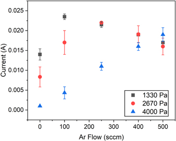
Figure 2. Measured current through substrate against Ar flow. At 1330 and 2670 Pa the peak current is at 100 SCCM and 250 SCCM Ar flow, respectively. At 4000 Pa the measured current increases with Ar flow.
Download figure:
Standard image High-resolution image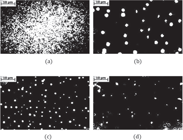
Figure 3. Binary images showing nucleation density corresponding to experiments 1–4 done at 1330 Pa. Black background is the silicon substrate and white represents boron-rich nucleation. Nucleation density is calculated by counting number of nuclei per unit area using ITCN in ImageJ. (a) Experiment 1: (b) Experiment 2, (c) Experiment 3, (d) Experiment 4.
Download figure:
Standard image High-resolution imageThe results of analyzing the film using glancing-angle XRD are shown in figure 4. The pattern shows broadened peaks, indicative of a disordered or nanocrystalline nature. Diffraction peaks from the silicon substrates are also present in the spectrum. The broad peaks are located at the same position of the prominent peaks for the B50C2 crystal structure, as provided in the Highscore plus software, reference code 96–1532749 and COD database code 1532748. This suggests a good match of our boron-rich film with a disordered B50C2 -type structure [27]. We have previously reported an MPCVD coating showing a similar disordered B50C2 structure [19]. Scanning electron microscopy of the surface of those coatings revealed densely packed rounded nodules consisting of a very-fine-grained morphology and Raman spectroscopy showed a combination of broad bands characteristic of an amorphous or a partially disordered structure. Therefore, the coatings are described as having a composite nature consisting of B50C2 nanograins in an amorphous matrix.
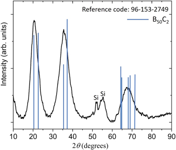
Figure 4. Glancing angle x-ray diffraction pattern of the boron-rich sample with best match to B50C2 phase. The blue lines show peak positions of the most prominent peaks associated with B50C2 taken from the database in Highscore plus software, reference code 96–1532749 and COD database code 1532748.
Download figure:
Standard image High-resolution imageFigure 5(a) shows nanoindentation load/displacement data of the grown film. The indents were performed to a depth of 300 nm at 11 locations. The average hardness of over the indents was measured to be 31 GPa with standard deviation of 15 GPa. Three measurements exhibited hardness greater than 40 GPa, which is in superhard regime. The indent with highest measured hardness was 58 GPa and had Young's modulus of 570 GPa. The average Young's modulus of this sample is 368 GPa. The relative contribution of elastic and plastic deformation can be calculated from the final unloading depth of the load-displacement curves. A high elastic recovery (about 67%) from the amorphous boron carbide sample is measured from the unloading data. Figure 5(b) shows the spread in the hardness data. Factors which are likely to influence this spread include sample surface roughness and non-homogeneity in material properties at the scale of nanoindentation.
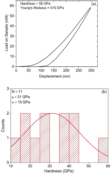
Figure 5. (a) Nanoindentation load-displacement curve from one location on the boron-rich sample to a depth of 300 nm. The measured values of nanoindentation hardness and Young's modulus are also indicated. (b) Histogram from 11 indents showing a mean hardness value for the boron-rich sample of 31 GPa.
Download figure:
Standard image High-resolution imageScanning electron microscopy (SEM) was used to image the surface morphology of the boron carbide coating grown using the optimal bias-enhanced nucleation stage. Low magnification in figure 6(a) shows a very dense and fine-grained microstructure. At higher magnification seen in figure 6(b), uniform ∼100 nm spheroidal particles are revealed. This coating, grown after bias-enhanced nucleation, yields much higher particle density with finer particle size than that reported in our previous study in which boron carbide coatings were grown without the bias-enhanced nucleation stage [19]. This also supports the effect of bias on nucleation density shown by the optical images in figure 3.
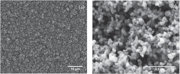
Figure 6. Scanning electron microscopy images of boron carbide coating at (a) low and (b) high magnification.
Download figure:
Standard image High-resolution image4. Discussion
 is directly proportional to the flux of ions bombarding the substrate per unit area [28]. There are other species in the plasma that act on the substrate. However, table 2 shows that Ts changes with bias voltage at constant H2/Ar flow rate (500 SCCM/100 SCCM) for each pressure. The substrate temperature, Ts, (normalized to the maximum measured value) plotted versus Ar flow is shown in figure 7 for −250 V. The observed trend for each Ts profile is similar to that observed for the bias current as shown in figure 2. Therefore, a peak in current measured through the substrate is due to a peak in the flux of ions bombarding the substrate, as evident by Ts.
Table 2.
 increases with bias voltage because ions are accelerated towards the substrate.
| Pressure (Pa) | Bias voltage (−V) | Ts (°C) |
|---|---|---|
| 150 |

| |
| 1330 | 200 |

|
| 250 |

| |
| 150 |

| |
| 2670 | 200 |

|
| 250 |

| |
| 150 |

| |
| 4000 | 200 |

|
| 250 |

|
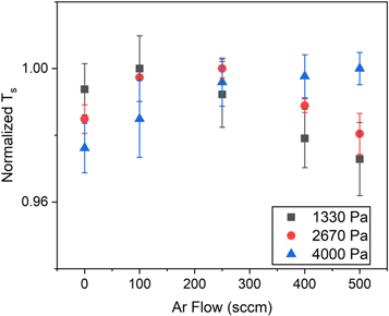
Figure 7. Normalized substrate temperature during Ar/H2 plasma plotted versus Ar flow at – 250 V. For 1330 and 2670 Pa, the peak substrate temperature occurs at 100 SCCM and 250 SCCM Ar flow, respectively. At 4000 Pa the substrate temperature shows no discernable peak in the Ar flow rate range tested.
Download figure:
Standard image High-resolution imageFigure 8(a) shows an OES spectrum of the plasma between 300 nm and 900 nm. 
 and
and  lines are seen at 434 nm, 486 nm and 656 nm, respectively. Several Argon emission lines are found between 696 nm and 840 nm, of which the line at 750 nm is most intense.
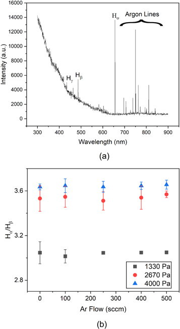
Figure 8. (a) OES spectrum between 300 nm and 900 nm showing H and Ar emission lines. (b)Ratio of Hα to Hβ is constant at each pressure 1330, 2670 and 4000 Pa.
Download figure:
Standard image High-resolution imageThe ratio of intensities of  to
to  from OES can be used to estimate the plasma electron temperature [29]. The ratio of
  to
to  remains constant at each pressure, shown in figure 8(b).
Quantitative values of the electron temperature can be obtained using the following two equations [30].


 and
and  are the emission intensity of
  and
and  respectively.
  is an optical device factor [31, 32].
  and
and  are excitation rate constants for transitions
  and
and  respectively [33].
  and
and  are de-excitation frequencies for
  and
and  respectively [34]. P is the pressure in hecto-pascal and
  is the electron temperature in Kelvin.
  and
and  are quenching cross sections of
  by
by  molecules and of
  by H atoms [32].
  and
and  are quenching cross sections of
  by
by  molecules and of
  by
by  atoms [34].
  is the mole fraction of
  The optical device factor is not calculated here. Instead, a normalized plot of
  to its value at 4000 Pa (Te4000) is plotted for 1330 (Te1330) and 2670 (Te2670) Pa in figure 9.
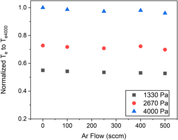
Figure 9. Electron Temperature in the plasma, normalized in terms of units of Te4000. Te1330 is about 0.54Te4000, and Te2670 is about 0.7Te4000.
Download figure:
Standard image High-resolution imageSince the MPCVD process categorically yields a 'cold' plasma, one can use an ideal gas law approximation [35, 36]. When the pressure and Te of the plasma are kept constant, adding Ar to the plasma should increase its volume. Photographs of plasma and its related image intensity have been reported to describe plasma volume [37, 38]. Figure 10 shows a photo of the plasma taken for the different flow rates of Ar and at different pressures. The image intensity of the plasma was analyzed by calculating the mean grey value of the plasma above the substrate, represented by the rectangle, using Fiji ImageJ. In figure 11, the normalized value of the image intensity of the plasma at each pressure is plotted versus the flow rate of Ar. Even with the unaided eye, it is observed that the plasma brightness drops off radially from its center and that it also extends to a larger volume as Ar flow rate increases. Based on this and that the measured image intensity decreases with increased flow rate of Ar at a point just above the substrate, we conclude that the plasma volume is increasing with increasing Ar flow rate and therefore it is likely that plasma species (including ions) are spread out over a larger volume.
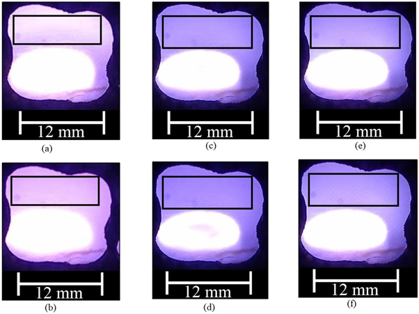
Figure 10. Photographs of plasma taken just above substrate. (a) 500 SCCM H2, 0 SCCM Ar, 1330 Pa. (b) 500 SCCM H2, 500 SCCM Ar, 1330 Pa. (c) 500 SCCM H2, 0 SCCM Ar, 2670 Pa. (d) 500 SCCM H2, 500 SCCM Ar, 2670 Pa. (e) 500 SCCM H2, 0 SCCM Ar, 4000 Pa. (f) 500 SCCM H2, 500 SCCM Ar, 4000 Pa.
Download figure:
Standard image High-resolution image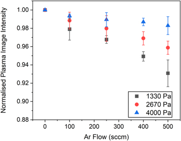
Figure 11. Normalized image intensity of plasma above silicon substrate as Ar flow varies.
Download figure:
Standard image High-resolution image
When the silicon substrate holder is negatively biased and the chamber of the CVD is grounded, as is the case in this set up, the direction of the electric field lines point toward the cavity walls [39]. For a given Ar flow rate, the plasma volume increases with decreasing pressure and more ions are spread away from the negatively charged substrate. Hence, these ions bombard the silicon substrate at a lower rate. At 1330 and 2670 Pa chamber pressure, this leads to a decrease in bias current associated with ion bombardment. As is evident from figure 10, the plasma intensity decreases (and therefore plasma volume increases) at a lower rate with increasing Ar for 4000 Pa as compared to that for 1330 and 2670 Pa. Therefore, the ions are not as exposed to regions of lower electric field, and the rate at which ions bombard the silicon substrate does not decrease. The net result is that there is no observed decrease in bias current with increased Ar flow for 4000 Pa chamber pressure in the Ar flow rate range investigated.
The rate of heterogeneous nucleation Ist is given in equation (3).:

Z is the Zeldovich factor, which is inversely proportional to the square root of Ts during nucleation [2]. Here, Ts changes primarily due to ion bombardment. We assume that Z is accounted for by Ts and study the effect of the other variables in equation (3) on nucleation density. kB is the Boltzmann constant. N is the number of atoms or molecules. During nucleation, the H2 and B2H6 flow rates are kept at 500 SCCM and 2 SCCM respectively. Therefore, N is kept constant during the 12 experiments in this study. K is the rate of molecule addition to a cluster of critical size. When a DC bias is used, ions are accelerated towards the negatively charged substrate, and thus K increases. Therefore, when only the DC bias changes between experiments, such as between experiment 1 and 2, or 3 and 4, for example (see table 1), the nucleation density increases.  is the critical work energy required for nucleation of a critical radius. Ar can be used to etch silicon. This increases the surface roughness of the silicon substrate and
  decreases. Therefore, when Ar is used in the plasma prior to nucleation changes between experiments, such as experiment 1 and 3, or 2 and 4, for example (see table 1), the nucleation density increases. At 1330 and 2670 Pa, the bias current through the silicon substrate is higher than at 4000 Pa. In this way, Ar is more effective at etching the silicon substrate at 1330 and 2670 Pa. We find that the nucleation density for experiments 1 and 5 are a factor of ten higher than the nucleation density for experiment 9.
 is inversely proportional to the rate of nucleation, and this is expected to affect nucleation density. Experiment 1 and 3, or 2 and 4, for example (see table 1), have similar
  since they have similar bias conditions. However, the measured value of nucleation density varies based on use of Ar to etch silicon substrate prior to nucleation. This indicates that changes in K and
  are more dominant than changes Ts in affecting nucleation density.
5. Conclusions
MPCVD with DC bias was optimized for highest current flow through a silicon substrate due to an Ar/H2 plasma at 1330 Pa. This current was analyzed for several Ar flow rates between 0 and 500 SCCM. Using optimized results found for 1330 Pa, silicon substrates were pre-treated with the DC bias in an Ar/H2 plasma. Control experiments were performed to evaluate the individual effect of using a DC bias and/or Ar in the plasma. These results show that nucleation density was 200 times higher when a silicon substrate is exposed to Ar/H2 plasma with DC bias than when the substrate is not exposed to Ar/H2 plasma and with no DC bias. Nucleation density was also tested at 2670 and 4000 Pa in order to evaluate the effect of pressure on the nucleation density while keeping other experimental parameters constant. When the substrate was pre-treated with a DC Bias in Ar/H2 plasma, both 1330 and 2630 Pa pressures showed similar nucleation densities which were nearly a factor of 7 higher than that for 4000 Pa. Results can be explained using an ideal gas approximation for the plasma and by incorporating OES measurements and basic heterogeneous nucleation theory. While bias-enhanced nucleation is commonly reported for carbon-based nucleation and growth, these results demonstrate that bias-enhanced nucleation is highly effective in synthesizing boron-rich deposits using MPCVD. The best pre-treated silicon substrate at 1330 Pa was used to grow boron-rich films which yielded amorphous boron-rich carbide with superhardness. The broadened peak of amorphous boron carbide is aligned with the prominent peaks of the B50C2 crystal structure from the database, suggesting that the amorphous sample is a disordered form of a B50C2-type structure. The average hardness of this sample is 31 GPa with values measured as high as 58 GPa.
Acknowledgments
This material is based upon work supported by the National Science Foundation (NSF) EPSCoR RII-Track-1 Cooperative Agreement OIA-1655280. Any opinions, findings, and conclusions or recommendations expressed in this material are those of the authors and do not necessarily reflect the views of the National Science Foundation.