
Abstract
The damages on silicon substrate, usually caused by machining and polishing processes, inevitably degrade the mechanical and electrical properties of the devices involved. Defect-free silicon substrates are essential with the miniaturization of integrated circuits to tens of nanometers, and repairing the damages is significant for manufacturing excellent devices. In this study, the slight damages, i.e. protrusive hillocks resulting from nanoscratching on monocrystalline silicon surface, was thermally annealed in vacuum for repairing, and groove-shaped scratches were also annealed for comparative study. In-situ topographies of the hillocks before and after the annealing were detected with an atomic force microscope (AFM), and then compared for finding the optimum annealing temperature. It is shown that the protrusive hillocks can be well repaired than the groove-shaped scratches. The repairing with annealing process was further verified by conductive AFM detection and selective etching in hydrofluoric acid solution. Raman spectroscopy detection was employed to clarify the annealing-dependent recovering mechanism of the damages on silicon surface, and it is suggested that structural transformation plays an important role in the repairing. In addition, the annealing of the hillocks on single-crystal quartz surface confirmed the structural recovery rather than the oxidation during annealing.
Export citation and abstract BibTeX RIS

Original content from this work may be used under the terms of the Creative Commons Attribution 4.0 licence. Any further distribution of this work must maintain attribution to the author(s) and the title of the work, journal citation and DOI.
1. Introduction
Owing to its excellent mechanical and physical properties, monocrystalline silicon has become the most popular material in semiconductors industry. It was widely used as a mechanical support and laid the foundation for modern electronic technology, integrated circuits, and optical components [1–3]. However, the destruction derived from manufacturing process can lead to the alteration and degradation in mechanical and electrical properties [4]. The defects can lead to the recombination of electron-hole pairs, which decreases the average carrier lifetime, and can also increase the current leakage and amplify noise [5]. Especially, the dislocation is one of the most harmful lattice defects in silicon causing the current leakage [6]. Besides, silicon substrates with amorphizations exhibit mechanical properties that differ significantly from defect-free silicon [7]. Therefore, eliminating these defects is of importance for improving silicon-based devices.
Nanoscratch on silicon surface by a diamond tip provided a simple approach to investigate the fundamental deformation behavior, because it was analogical to the damage in surface polishing and diamond machining processes [8, 9]. In the past few years, the investigations indicated that phase transformation and microdefect formation on silicon surface were two dominant phenomena associated with a scratching process [10]. Moreover, the deformation mechanisms on silicon surface during nanoscratching depend strongly on the loading conditions [11]. It was reported that the deformation sequence in nanoscratching was amorphous formation, stacking faults/twin development and full dislocations deformation with the increase of normal load [12]. Especially, when the contact pressure between diamond tip and silicon substrates is less than ∼11.3 GPa, the sliding of diamond tip can lead to the generation of protrusive structures, which can be viewed as pre-stage wear, instead of material removal [13–15]. Combining x-ray photoelectron spectroscopy and auger electron spectroscopy, oxygen content and its distribution in depth were detected from the hillock on silicon surface. Cross-sectional transmission electron microscope analysis showed that the formation of such protrusive hillocks can be mainly attributed to the amorphization, while oxidation provided limited contribution [14–16].
Heat treatment is a fundamental process in silicon wafer manufacturing. The annealing and oxidation process can reduce surface charges and silicon dangling bonds induced during the device fabrication, effectively enhancing device stability [17]. For instance, thermal annealing with the temperature of ∼1000 °C is widely applied for reversing the damage [18]. Also, in silicon-based luminescent structures design, it is found that the traces of scratches became less noticeable, and the densities of loops and dislocations slightly decreased after being annealed [19]. In addition, the mechanical strength of silicon can be expressed by the ability to resist dislocation movement [20], and more investigations were focused on enhancing the strength of silicon by annealing [21]. The dislocations in groove-shaped scratches can be minimized or eliminated by annealing in oxygen-controlled or nitrogen environment [22, 23]. Therefore, for the slight damages in the form of friction-induced hillocks caused by ultra-precision machining on silicon surfaces, thermal annealing was expected to become a possible method for repairing.
In this work, annealing treatments in vacuum were applied to repair silicon surface with slight damages, i.e. friction-induced hillocks and groove-shaped scratches. The effect of annealing temperature on surface topography evolution of the scratched surface was studied to ascertain optimum annealing condition. Scratches with different types of damages were annealed at the certain temperature for determining the repair effect of those damages. The repairing process was further verified by conductive atomic force microscopy (CAFM) detection and selective etching in hydrofluoric acid (HF) solution [24, 25]. Raman spectroscopy was employed to identify the phase transformation before and after the annealing. Finally, the morphological evolution of the hillocks on single-crystal quartz surface after being annealed further confirmed the damage repair induced by high-temperature annealing. This study may shed light on repairing damages of silicon surface and even slight damages of silicon-based devices by thermal annealing.
2. Materials and methods
The B-doped Si (100) wafers (Suzhou Research Materials Microtech Co., Ltd, China) with a resistivity of 10 Ω·cm grown by the Czochralski method (the oxygen and carbon are 8 ∼ 18 and <1 ppma), and single-crystal quartz (AT-cut) wafer (Hefei Kejing Materials Technology Co., Ltd, China) were used for the scanning tests. Moreover, all scanning tests were performed in vacuum using an AFM (E-Sweep, Hitachi Instruments Inc., Japan). The friction-induced hillocks with a length of 10 μm on silicon and quartz surface, which were prepared by a diamond tip (tip radius R ≈ 550 nm) under line-scanning mode. Besides, groove-shaped scratches were produced by a diamond tip (R ≈ 20 nm) under the normal load Fn of 10 μN. A pit with an area of 2 × 2 μm was prepared under area-scanning mode for the annealing and Raman spectroscopy analysis.
Thermal annealing was performed in a two-zone tubular furnace (OTF-1200X-II; Hefei Kejing Materials Technology Co., Ltd, China). During the annealing, the samples were first put into the insulated furnace cavities, and ∼99.999% argon was injected into the furnace chamber at a rate of 100 ml/min for 1 h from the air intake, resulting in that the internal air was squeezed out from the air outlet. Then, the samples with line scratches were annealed in vacuum with a pressure blew 4.0 Pa for 1 h (the holding time). After that, all samples were ultrasonically cleaned (the frequency of the ultrasonic wave is ∼40 kHz) in acetone, ethanol, and deionized water sequentially to eliminate potential surface contaminations. The in-situ topography evolution of scratched area before and after the annealing were detected by the AFM. For further investigating the annealing mechanism, the annealed samples were etched in 30 wt.% HF solution for 60 min at room temperature (∼25 °C), and all current images were in-situ gathered at −2 V bias by conductive AFM. The thickness of the silicon oxide layer was evaluated by an Ellipsometry (EMPro, Beijing saifan Photoelectric Instrument Co., Ltd, China) using 632 nm wave with incident angle of 68°. The scratched area before and after being annealed was detected with a Raman imaging microscope (Nano XploRA, Horiba France SAS, France) by using 632.8 nm excitation line from a helium-neon laser.
3. Results and discussion
3.1. Temperature-dependent annealing of friction-induced hillocks
Figure 1 shows AFM images of hillocks with the height of ∼5 nm created under the same loading condition on silicon surface before and after being annealed in vacuum. The images of the original and annealed hillocks at 500, 900, and 1000 °C were displayed in figure 1(a). Obvious decrease in the height of the hillocks was detected from the topographies after the annealing, and higher temperature annealing can lead to rapider decrease in height of the hillocks. After being annealed at 1000 °C, the height and dimension of the hillock have been significantly reduced, and the hillock nearly as flat as the silicon surface. The cross-sectional profiles of the hillocks before and after being annealed at various temperatures were compared in figure 1(b). The hillocks became lower and narrower with the increase of annealing temperature, and the heights decreased 24% to 90% after being annealed at 500, 700, 900, 1000, and 1100 °C, respectively. It is also worth noted that hardly any difference could be detected between the hillocks annealed at 1000 and 1100 °C. Hence, one can infer that the optimum annealing temperature can be ∼1000 °C for the friction-induced hillocks on silicon surface.
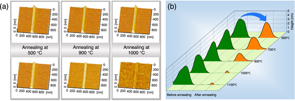
Figure 1. The friction-induced hillocks annealed in vacuum at various temperatures. (a) AFM images of the hillocks (Fn = 20 μN and sliding velocity v = 10 μm s−1) before and after being annealed at 500, 900, and 1000 °C, respectively. (b) Cross-sectional profiles of original hillocks and annealed ones at 500, 700, 900, 1000, and 1100 °C, respectively.
Download figure:
Standard image High-resolution image3.2. Repairing scratch damages under light load by annealing
The annealing in vacuum at 1000 °C was employed to repair the scratch damages under different processing conditions. Figure 2 shows AFM images of friction-induced hillocks and a groove on silicon surface, where the hillocks were produced under different sliding velocities from 1 to 1000 μm s−1. The height of hillocks produced under low velocity was higher than that under high velocity. It was found that the lower sliding velocity was beneficial to amorphous deformation, which contributed significantly to the height of hillocks, while the higher sliding velocity is conductive to the formation of deformed silicon, including dislocations and stacking faults [15]. After being annealed, both height and width of the two hillocks decreased gradually, and the hillock produced at 1000 μm s−1 even returns completely to the original surface (see figure 2(a)). Besides, the groove in figure 2(a) was prepared under a higher pressure beyond 11 GPa based on the Hertz contact model [26]. It can be inferred that there was a large amount of residual stress and plastic deformations in the original groove. After being annealed, the depth of the groove decreased from 8 nm to 4 nm. This may be attributed to the structural recovery caused by the residual stress reduction, which was greatly reduced by a small degree of dislocation propagation at a temperature above 500 °C as reported [27]. Comparing the repair between the hillock and the groove, a deep vestige left on silicon surface after the groove being annealed, while the hillock can be significantly recovered and with a few residues. The annealing of the hillocks under various sliding velocities are shown in figure 2(b). Compared with the original height of the hillocks produced at various velocities (1, 10, 40, 100, 400, and 1000 μm s−1), the height of annealed hillocks decreased 79% to 68%.
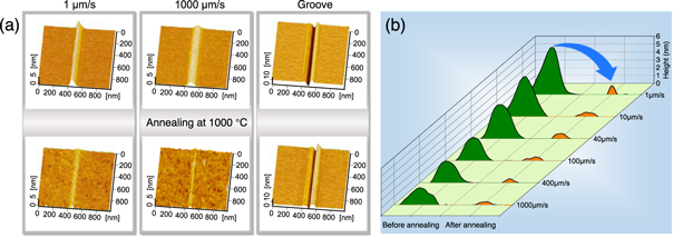
Figure 2. Thermal annealing of friction-induced hillocks and a groove on silicon surface at 1000 °C. (a) AFM images of two hillocks and a groove before and after being annealed. (b) Cross-sectional profiles of a series hillocks before and after being annealed. The hillocks were produced with a diamond tip (R ≈ 550 nm) under Fn = 20 μN, and v was from 1 μm s−1 to 1000 μm s−1 (marked beside the figures). The groove was produced with a diamond tip (R ≈ 20 nm) under Fn = 10 μN and v = 1 μm s−1.
Download figure:
Standard image High-resolution imageThe illustrations of hillock volume and recovery ratio p evolution were plotted to further indicate the recovery effect of friction-induced hillocks during the annealing. The change in hillock volume at various annealing temperatures was presented in figure 3(a). It can be illustrated that the hillocks produced under the same conditions presented quite similar volumes, and the volumes of the hillocks after being annealed decreased with the increase of annealing temperature. Specifically, when the annealing temperature increased from 500 to 700 °C, the volume started to decrease, while p rose slowly. As the temperature rose to 1000 °C, the volume decreased rapidly, and p raised from ∼0.4 to ∼0.9. When the temperature was beyond 1000 °C, p kept at ∼0.9. In other words, with the increase of annealing temperature, p increased rapidly, while p kept basically stable after the temperature reaches 1000 °C. Considering that there was no material addition or removal throughout the process, it may be referred that the amorphous region in hillocks is a loose and expanded structure, which can be recovered to some density structures and down to the original silicon surface after 1000 °C annealing.
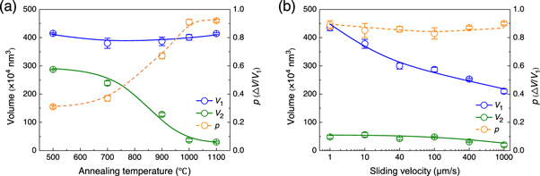
Figure 3. Effects of (a) sliding velocity and (b) annealing temperature on hillock volume and recovery ratio p. In this study, p is expressed as ∆V/V1, where ∆V = V1–V2. V1 and V2 represent the volumes of hillocks before and after being annealed, respectively.
Download figure:
Standard image High-resolution imageThe change trend in the volume of annealed hillocks produced at various sliding velocities were shown in figure 3(b). It can be observed that the volume of the original hillock decreased with the rise of sliding velocity. After being annealed at the same conditions, the volumes of all hillocks decreased obviously, and kept almost stable consistent regardless of processing velocity. Moreover, p of the hillocks prepared under various sliding velocities maintained at ∼0.9. Therefore, although there were different damage types of the hillocks formed at various velocities [15], the recovery ratio was nearly consistent after being annealed.
3.3. Current changes in annealed silicon of line-scanning mode
It was reported that CAFM images presented obvious electrical breakover signals on scratched silicon area, which was attributed that lattice distortions, including dislocations, stacking faults and slips, can facilitate the electron flow compared to monocrystalline silicon and amorphous silicon [24]. This phenomenon can be used to determine the transformation of those damages in the scratches after being annealed. Figure 4(a) displays the surface topographies and current images of a hillock prepared under a velocity of 1000 μm s−1 before and after being annealed. Current breakover signals can be observed in the hillock, and the maximum current was measured as ∼26 pA. After being annealed at 1000 °C, the height of the hillock decreased from 2.7 nm to 0.8 nm, and the current breakover signals can hardly be detected from the annealed hillock. By comparison, the current evolution of the groove by thermal annealing had been further investigated for addressing the recovery. As shown in figure 4(b), a maximum current of ∼60 pA can be detected from the groove with the depth of ∼8 nm. After being annealed, the groove depth reduced to ∼4.5 nm, and a current of ∼25 pA still can be gathered. This may be due to the recrystallization of amorphous silicon on the surface after being annealed [28, 29]. After being annealed, no current signals were gathered in the hillocks, while the obvious current signals can be detected from the groove.
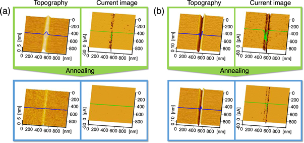
Figure 4. Surface topographies and corresponding current images of (a) a friction-induced hillock and (b) a groove on silicon surface before and after being annealed at 1000 °C. The hillock in (a) was produced by a diamond tip (R ≈ 550 nm) under Fn = 20 μN and v = 1000 μm s−1, and the groove in (b) was created by a diamond tip (R ≈ 20 nm) under Fn = 10 μN.
Download figure:
Standard image High-resolution image3.4. Chemical and structural analysis
The thickness of the silicon oxide layer was evaluated by the Ellipsometry. By using the same conditions for the annealing, the thickness of the silicon oxide layer after being annealed at 700 and 1000 °C is 21.3 and 76.1 nm, respectively. The result indicates that serious oxidation occurred on the silicon surface during the annealing. Various methods were adopted to remove oxygen in the early stage of the annealing; however, the oxidation can never be avoided. From test results on the oxide thickness, it is believed that the oxidation also contributes to the recovery.
The amorphous silicon can be etched by HF solution whereas the crystalline silicon withstands etching [25]. In this study, the thickness of the amorphous phase was estimated by HF solution etching, which can be used to reflect the transformation of the amorphous phase after being annealed. As shown in figure 5, an original hillock with the height of ∼5 nm was treated directly in HF solution for 60 min, the hillock transformed to groove with the depth of ∼6 nm. The thickness of the amorphous phase in this hillock can be considered about ∼12 nm. For comparison, another hillock with the same height produced under the same sliding conditions was annealed in vacuum at 1000 °C. The height of the hillock decreased to ∼0.7 nm. Then, the annealed hillock was placed in HF solution for 60 min, only a smooth groove with depth of ∼0.3 nm was detected. The removed part on the annealed hillock was ∼1 nm thick. A thin layer of silicon oxide will be formed on the hillock surface during the processing, and this oxide will change hardly during the annealing. Moreover, HF solution is often used in silicon wafer cleaning and pattern delineation by etching silicon dioxide [30]. Hence, the removed part with the thickness of ∼1 nm may be regarded as silicon oxide of this part. Compared with the amorphous phase with the thick of ∼12 nm, these silicon oxides were negligible, and most of the amorphous phase was transformed during annealing. It may infer that the amorphous phase was repaired into a structure like the surrounding silicon surface to resist HF etching.
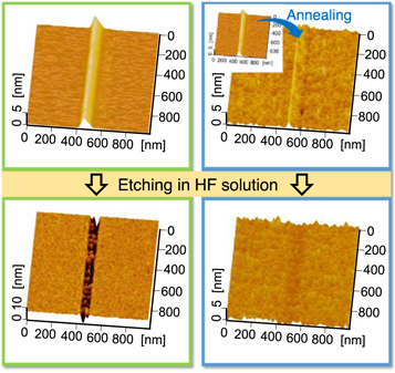
Figure 5. AFM images of an original hillock (left panel) and annealed hillock at 1000 °C (right panel) before and after being etched by 10 wt.% HF solution for 60 min.
Download figure:
Standard image High-resolution imageRaman spectroscopy was employed to identify the phase transformation of the scanned area on silicon surface after high-temperature annealing. Figure 6 illustrates the in-situ Raman spectra which were collected on the groove before and after being annealed, as well as the pristine silicon surface for comparison. On all spectra, the single band at 521 cm−1 can be observed, close to the reported 520 cm−1 optical mode of bulk silicon (Si-I). From the spectra, it can be inferred that the scratched area was composed of Si-I, amorphous silicon (a-Si, 470 cm−1), high-pressure phase Si-XII (491 cm−1), and Si-III (415, 447, and 465 cm−1). It should be noted that the band at 475 cm−1 was also identified as amorphous silicon [31]. However, the intensity of the band of Si-III was very low on the original scratched surface, corresponding to low content of Si-III structure. Both Si-III (bc8, body-centred cubic structure [32]) and Si-XII (r8, the rhombohedral distortion of bc8 [33]) are known to show semi-metallic electronic behaviors [34], which may result in the generation of current breakover signals in the scratched area (see figure 4). Considering that the current intensity on the hillock is lower than that on the groove (see figure 4), this indicated that there were few lattice distortions excluding amorphous layer in the hillocks, while the dislocations or cracks in the groove contributed a lot to current signals.
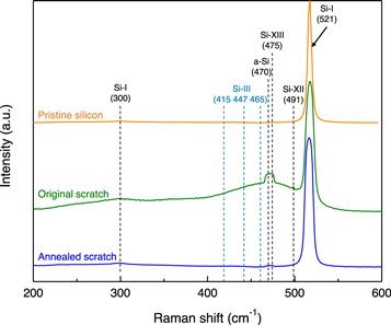
Figure 6. Raman spectra of a groove (original scratch) and a groove annealed in vacuum at 1000 °C (annealed scratch), as well as native silicon surface (pristine silicon).
Download figure:
Standard image High-resolution imageAfter being annealed, the polymorphs had basically vanished, and the characteristic band of bulk silicon was observed as shown in the spectra of annealed scratch (see figure 6). The characteristic band of metastable phase Si-III and Si-XII can be hardly observed on the annealed scratch, which is consistent with that the Si-III/XII → Si-I phase transition occurs at 500 °C. The metastable silicon phases (Si-III and Si-XII) will be transformed into thermodynamic stable Si-I at high-temperature annealing [35]. Therefore, the thermal annealing method in a vacuum furnace at 1000 °C could be used to repair those damages. In addition, it is also noted that the peak of the amorphous silicon band decreased greatly compared to that without annealing, corresponding to the evidence of the annealed hillock resistance to HF etching, and this may due to a-Si → Si-IV → Si-I phase transition after high-temperature annealing [36].
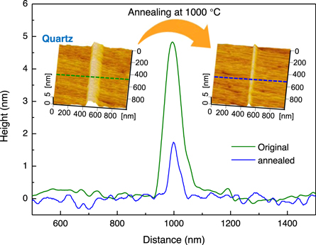
Although the air in the furnace chamber was replaced by high purity argon and the vacuum treatment was carried out before annealing, the extremely little oxygen may remain, resulting in the oxidation of sample surfaces to some extent. To verify the structural recovery by annealing, the annealing of friction-induced hillocks on the single-crystal quartz, which consists completely of silicon oxide and hardly reacts with the oxygen, was carried out. As shown in figure 7, the hillock with the height of ∼5 nm was prepared under the contact pressure of ∼6.3 GPa, and then the quartz sample was annealed in vacuum at 1000 °C. Similarly, the height of the hillock on quartz surface decreased to ∼1.7 nm. The p of friction-induced hillocks on quartz surface during the annealing was measured as ∼0.8, which is lower than that on silicon surface (∼0.9) (see figure 3). After being annealed at high temperature, it is noticed that the hillocks decreased greatly on the single-crystal quartz, which could be attributed to the recrystallization of the amorphous phase. Furthermore, it is confirmed that structural recovering plays an important role in the repairing of damages on the monocrystalline silicon surface. However, the oxygen cannot be removed completely because of the large space of the furnace chamber and the adsorbed oxygen in the crevices [37]. The residual oxygen can cause the oxidation of surface nanostructures especially at high temperature (as verified by the Ellipsometry test). A further investigation to avoid or reduce greatly the impact of the oxidation is needed for advancing the recovery mechanism of nanoscale damages by the annealing.
Figure 7. AFM images and its corresponding cross-sectional profiles of a friction-induced hillock on single-crystal quartz surface before and after being annealed in vacuum at 1000 °C.
Download figure:
Standard image High-resolution image
4. Conclusions
As the pre-stage of wear, friction-induced hillock on monocrystalline silicon surface is composed of extensive amorphous structures and little lattice distortions. The annealing in vacuum was introduced to repair the damages in the present study. The height of friction-induced hillocks can be reduced significantly after being annealed at the optimum temperature of 1000 °C, and the recovery ratio of the volume can reach ∼0.9. By CAFM detection and HF selective etching, the hillocks after being annealed showed similar performances as the original silicon surface. Raman spectroscopy analysis further demonstrated that the recovery of the damages was partly ascribed to the phase transformation by thermal annealing. Besides, the repairing of slight damages on the quartz surface also verified the structural recovering during the annealing. In summary, slight damages, especially friction-induced hillocks, on the monocrystalline silicon surface can be repaired by thermal annealing, and electrical and chemical properties can be recovered to its original states to some extent. Furthermore, structural repairing plays an important role in the whole repairing progress compared to the oxidation during annealing. This study may shed light on repairing damages on silicon surface and even slight damages of silicon-based devices by thermal annealing.
Acknowledgments
The authors would like express thanks to the supporting by the National Natural Science Foundation of China (51775462 and 51991371).
Data availability statement
All data that support the findings of this study are included within the article (and any supplementary files).