

Abstract
Indium nitride is one of the very few semiconductors which is known to have a superconducting phase at temperatures of Tc > 1 K. Superconductivity occurs in a window of carrier densities of approximately 1018–1020 cm−3. This is a very low density when compared to other superconductors (i.e. metals, alloys, high Tc oxides) and thus raises interesting fundamental questions as well as technological possibilities. In this paper we address one key question about the dimensionality of the superconducting state of InN by using angle dependent critical field measurements. Our samples were grown by two different growth techniques (chemical vapour deposition and plasma-assisted molecular beam epitaxy) on c-oriented sapphire, with and without a GaN buffer layer. In both cases we find that for film thicknesses much larger than the coherence length d ≫ ξ, the angle dependence of the critical field (down to T < 280 mK) with respect to the c-axis continues to be clearly two-dimensional, demonstrating a characteristic cusp when the angle crosses 90° with respect to the c-axis. This indicates that the superconducting electrons are most likely confined to a layer much thinner than the thickness of the InN film. Further we find the magnitude of the gap to be 2Δ(0)/kBTc = 3.6, very close to the BCS prediction.
Export citation and abstract BibTeX RIS
The prospect of robust superconductivity at low carrier densities raises several interesting questions. On one hand screening and condensation mechanisms in interacting many body systems at low densities, potential Fermi-surface instabilities etc. are of fundamental interest. At the same time it opens up technological possibilities like field effect control of superconducting channels and junctions that would be fundamental to superconducting electronics. Elemental metals and various alloys have carrier densities nc ∼ 1023 cm−3, well known high Tc oxide superconductors have nc ∼ 1021 cm−3. For lower carrier densities it is quite natural to look in semiconductors, where 1016–1020 cm−3 carrier densities are common. There is however no known observation of superconductivity significantly below 1018 cm−3. Historically GeTe was the first such system to be reported with a transition temperature Tc ∼ 100 mK [1, 2]. In the following 50 years only a few more were reported: B doped diamond [3], B doped cubic Si [4] and InN [5]. InN attracted considerable attention in last 10–15 years, [6–17] because unlike GeTe which has very low critical temperatures and critical fields, data from InN films show a transition at Tc ∼ 2–3 K, which is more easily achieved. The doping (worked out from Raman spectra) at which diamond and Si show superconductivity is above 1021 cm−3, a number almost comparable to the carrier concentration of normal metals. In case of InN data available so far suggest that a carrier density of ∼1018 cm−3 is sufficient. It is however somewhat puzzling, that no clear and systematic variation of Tc with the carrier density has been noticed. The mechanism of superconductivity in InN remains a matter of some debate. Initial investigators did not rule out the possibility of phase segregated clusters of indium, weakly coupled but percolating the system, giving rise to the effect. But the observed critical fields were far too high to result from clusters of metallic superconducting indium (μ0Hc(T = 0) = 0.03 Tesla). Later work brought up this possibility again by showing that Ginzburg's analysis of superconductivity in few nanometer sized grains does allow for significant enhancement of Hc. Experimentally observed Shubnikov–de Haas oscillations however appear to establish that the grain sizes are not smaller than the cyclotron radius (∼100 nm) [8]. One school of thought ([6, 7, 9, 18]) has suggested that polarization reversal (inversion domain) occurs in wurtzite unit cell of InN due to the weak force constant along c-axis, some In atoms exchange their position with N atoms. As a result, In–In chains with a bond length of 2.14 Å are produced in the ![$[11\bar{2}0]$](https://content.cld.iop.org/journals/0953-2048/32/1/015009/revision2/sustaaed8fieqn1.gif) direction of the lattice. When the length of these In–In chain is longer than the coherence length of In (∼70 nm) then InN shows superconductivity, thus it is intrinsic. But some authors have attributed the superconductivity in InN to (not intrinsic) presence of oxygen impurity [14]. However, questions concerning the nature of superconductivity in InN still remain.
direction of the lattice. When the length of these In–In chain is longer than the coherence length of In (∼70 nm) then InN shows superconductivity, thus it is intrinsic. But some authors have attributed the superconductivity in InN to (not intrinsic) presence of oxygen impurity [14]. However, questions concerning the nature of superconductivity in InN still remain.
InN thin films used in this work, were grown on sapphire substrate by two different techniques—chemical vapour deposition (CVD) and plasma-assisted molecular beam epitaxy (PA-MBE) on c-oriented sapphire. The CVD was carried out using pure indium metal and ammonia as precursors [19, 20]. For PA-MBE samples, first a buffer layer of GaN was deposited on sapphire substrate and then InN was grown on GaN using PA-MBE system [21]. The role of various growth parameters, structural studies, cross-sectional analysis, epitaxial relationships between the film and the substrate, width of the transitions etc have been reported by us in [19, 21] and [22]. We note that the absence of oxygen O1s core level transition in XPS (and hence negligible oxygen impurity) was also demonstrated for the PA-MBE samples in [21]. The details are summarised in table 1. However we do not reproduce the structural analysis data here, since these have already been reported. Notice that the carrier densities of the films differ by nearly a factor of 100 from 5 × 1018 cm−3 to 4 × 1020 cm−3 and the mobilities differ by more than a factor of 10. In this paper we focus on the angle dependent four-probe magnetotransport experiments, carried out in a cryostat where the sample could be rotated in situ allowing the angle between the direction of the magnetic field and the c-axis to be varied continuously. The cryostat used for these measurements was a sorption pumped He-3 system, where base temperature ≈250 mK could be reached. Preliminary observations of large critical fields and quasi-2D behaviour were reported earlier [22]. Due to the absence of Schottky barrier at the surface of InN (similar to InAs) ohmic contacts did not require any annealing. Both indium dots and evaporated Ti/Au contacts gave similar results as expected. The linearity of the current voltage characteristics were carefully checked for the contacts at room temperature as well as the lowest temperature to confirm the absence of a Schottky barrier.
Table 1. The summary of InN thin film parameters. Tc0 is the mean-field transition temperature. The details of the growth methods (CVD and PA-MBE paramters like gas flow rates, substrate temperatures etc) and structural studies have been reported earlier in [19–22] and are not repeated here. The thicknesses reported here are the targeted thicknesses during the growth process. We carried out profilometer measurements on the samples after etching the Hall-bar patterns. The measured values were within 5%–10% of the 'target' values.
| Sample | Thickness | Tc0 | nc | μ (300 K) |
|---|---|---|---|---|
| I.D. | (nm) | (K) | (cm−3) | (cm2 V−1 s−1) |
| IN12TF01 | Sapphire/InN | 2.47 | 3.37 × 10²⁰ | 36.22 |
| (CVD) | 200 | |||
| IN01TF01 | Sapphire/InN | 2.48 | 4.11 × 10²⁰ | 75.20 |
| (CVD) | 200 | |||
| IN08TF01 | Sapphire/InN | 1.80 | 2.57 × 10²⁰ | 36.70 |
| (CVD) | 200 | |||
| B31 | Sapphire/GaN/InN | 2.98 | 1.63 × 10¹⁹ | 187.67 |
| (PA-MBE) | 300/300 | |||
| B36 | Sapphire/GaN/InN | 2.25 | 2.67 × 10¹⁹ | 92.8 |
| (PA-MBE) | 300/300 | |||
| B32 | Sapphire/GaN/InN | 2.39 | 1.29 × 10¹⁹ | 133.96 |
| (PA-MBE) | 300/300 | |||
| G09 | Sapphire/GaN/InN | 1.98 | 5.52 × 10¹⁸ | 403.28 |
| (PA-MBE) | 300/300 |
Table 2. Values of coherence length and superconducting layer thickness calculated from Hc(θ).
| Sample | ξ(0) (nm) | dS (nm) | Sample | ξ(0) (nm) | dS (nm) |
|---|---|---|---|---|---|
| IN12TF01 | 34 | 67.7 | B31 | 18.5 | 26.3 |
| IN01TF01 | 35.7 | 50.7 | B36 | 26 | 27 |
| IN08TF01 | 37.5 | 72.3 | B32 | 28.4 | 40.6 |
| G09 | 40 | 85 |
The temperature dependence of sheet resistances for all the samples (in zero magnetic field) are summarised in figure 1. Notice that the  (i.e. insulating) behaviour is also seen in low carrier density samples although all the samples are superconducting at low temperatures. We observed that the resistive transition was in general sharper in the PA-MBE samples with higher mobilities.

Figure 1. Temperature dependence of sheet resistance RS of all the samples. Notice that the PA-MBE samples have higher mobilities but lower carrier densities, possibly on account of lesser number of defects which provide the conduction electrons. All resistance measurements were done in four-probe geometry, using a low frequency a.c. lock-in amplifier technique (f = 127 Hz). The sheet resistivities (RS) were calculated by using the Van der Pauw formula.
Download figure:
Standard image High-resolution imageElectrical transport in superconducting thin films depends strongly on the relative magnitudes of the thickness d of the film and the coherence length ξ. Figure 2 summarises the resistive transition data in perpendicular magnetic fields from which one may deduce the coherence length. The upper critical field  at a given temperature is taken to be the magnetic field at which the resistance reaches half its normal state value. The transition temperature in a given field is defined as the temperature that corresponds to the mid-point of the resistance trace (figure 2(a)). The temperature dependence of critical field is determined from the graph as shown figures 2(c) and (d). The curvature of the traces is such that ,
  cannot be fitted with the empirical relation of Gorter–Casimir two-fluid model [23],
where ϕ0 = h/2e is the flux quantum (SI units). The extrapolated values of  for CVD grown samples are seen to be in the range from 0.14–0.27 T and the value of
  is larger as expected, ranging from 0.26–0.46 T. For MBE grown samples, the value of
  is seen to be between 0.5–1.2 T. The
  values clearly indicate a coherence length ξ ≈ 20–40 nm (see table 2). The thickness of the InN layer (d) is at least five to ten times larger than that. This would in general indicate that the d ≫ ξ should be the appropriate regime. It is also clear from figures 2(c) and (d) that a plot of Hc(T)/Hc(0) versus T/Tc does not cause all the data to collapse on a single curve. We have tried to fit it (figure 2(b)) with the theory of single band, dirty Type-II superconductors, the Werthamer–Helfand−Hohenberg (WHH) model) [24], without much success (figure 2(b)).

Figure 2. (a) The resistive transitions in a magnetic field, B⊥ab plane. The dotted line shows the value RN/2. Notice that the magnetoresistance in the normal state is negligible. Thus there is no difficulty in determining the value of magnetic field at which the RN/2 point is reached. Thus within the mean-field definition the error in determining the the critical field is negligible and not shown (i.e. as error bars). (b) The critical field can be fitted with the Tinkham model only in certain cases. C–G refers to the Cassimir-Gorter model, WHH refers to the Werthammer–Helfand–Hohenberg model. (c) The evolution of Hc2(T) with carrier density for the B⊥ab plane and (d) for the B∥ab plane.
Download figure:
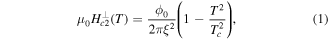
Standard image High-resolution imageIf we now consider the regime in which the thickness of the superconducting layer is smaller than the coherence length d < ξ following Tinkham's 2D model [25–27] the prediction for the critical magnetic field dependence for the ( ) would be:
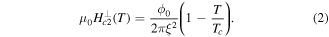
Further the effective thickness of the superconducting layer (dS) is related to  as
as
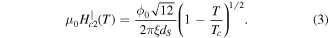
Using Hc2(θ) data and equations (2) and (3), ξ and dS can be determined. We get good agreement with this model as shown in figure 2(b) for relatively higher carrier density samples. For IN08TF01,the extrapolated value of critical field is around 0.25 T and calculated in plane coherence length is ≈37 nm. However it is also to be noted that the curvature of the  as seen in figure 2 bottom inset is slower than linear and is not accounted for by equation (2). However a clear conclusion can be drawn from the data obtained from the dependence of the critical field on the angle it makes with the substrate. The 2D or 3D nature should show a distinct difference. The 3D model is anisotropic Ginzburg–Landau (G–L) model [28–30] and according to this model, the critical field depends on the angle between the superconducting layers and applied field by the equation,

where θ is the angle the magnetic field makes with the c-axis of the sample.
The 2D model is Lawrence–Doniach (L–D) model [25, 31] and according to this model, there is a weak coupling between the superconducting layers in the 2D limit. The equation for angle dependence of critical field by the L–D model is
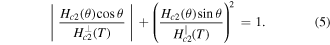
We note that in literature the 2D model cited here appears to be have been referred to as either Tinkham or the L–D model somewhat interchangeably by various authors [13, 32, 33]. Figure 3 shows data from two samples in detail. All other samples too showed very similar characteristics. The difference between the prediction of the 3D G–L and 2D L–D model is that in the 2D case the magnitude of the critical field exhibits a sharp cusp when the magnetic field makes an angle of 90° with the c-axis. In our data a cusp-like feature at 90° is clearly observed even though the film thickness d ≫ ξ, indicating that the superconducting electrons may be confined to a very thin layer. Using equations (2) and (3) we find dS ≈ 25 nm for B36, which is more than ten times less than the physical thickness of the layer. Similar results are obtained from other datasets. InN and InAs are both low bandgap semiconductors which do not form a Schottky barrier at the surface with metal contacts due to a large density of surface states. X-ray and ultra-violet photo-emission data also support the presence of a large electron concentration near the surface [20]. It is possible that it is this quasi-2D layer, with the polarisable lattice of InN and the other free electrons providing a suitable dielectric function, that goes superconducting.

Figure 3. (a) The angle dependence of critical field of PA-MBE grown patterned InN (B36) (b) The angle dependence of critical field of CVD grown InN (IN08TF01). Table 2 shows values of ξ(0) and superconducting layer thickness (dS) calculated from Hc(θ).
Download figure:
Standard image High-resolution imageThere seems to be a systematic evolution from upward curvature to linear temperature dependence in as the density increases. It has been shown theoretically [34] that in a dirty superconductor, Hc2 can be enhanced at low temperatures and may even show upward curvature due to the localization of electrons and suppressed density of state at low temperature. Experimentally (in Al films) the authors of [35] have shown that in a dirty superconductor, that instead of a downward curve in Hc2, a linear or even an upward curve of Hc2 may arise. However this aspect would require more careful analysis.
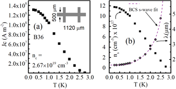
Our measurement of the critical current density (Jc), with the assumption that the supercurrent is confined to a cross section dS as calculated earlier, and not d, (the physical thickness of the film) is shown in figure 4(a).
Figure 4. (a) The measured values of the critical current Jc. (b) The calculated superconducting carrier density ns (left scale) and the penetration depth, λ(T) (right scale). The dotted line is the fit to λ(T) using equation (7).
Download figure:
Standard image High-resolution image
For thin films of type-II superconductors with thickness d < λ, Jc is given by

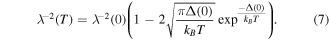
where κ(T) = λ(T)/ξ(T) is the Ginzburg–Landau parameter, has very little temperature dependence and can be effectively treated as constant under the logarithm. Using equation (6) the value of λ(T = 0) can be calculated first by using the already calculated ξ(0). Treating the term inside the logarithm as approximately constant we find λ(T). For type-II superconductors like InN this provides a simple means to extract absolute values of λ(T) and, from its temperature dependence, the symmetry and magnitude of the superconducting gap [36].
The results are summarised in figure 4. Jc(0) ≈ 108 A m−2 imply a penetration depth λ(0) ≈ 1.7 μm. The super-electron density ns can then be calculated as λ = (m*/μ0nse2)1/2. For InN the band effective mass, m* ≈ 0.1 m0, where m0 is the free electron mass. The saturated ns at 270 mK is then ≈1018 cm−3, which is about 4% of the normal electron density of the sample from Hall data. The energy gap has been determined from fitting the low-T behaviour of λ(T) as shown in figure 4. For s-wave symmetry:
The fit gives Δ (0) = 330 ± 2.5 μeV and hence  in close agreement with the BCS value without any disorder correction. It is interesting to ask how these conclusions would have been modified if the physical thickness of the film (200–300 nm) was used to convert the measured critical currents to current densities. We found that although it results in a change of the absolute value of λ, it does not change the nature of the temperature variation. Equation (7) requires one to know only the nature of variation of λ(T)/λ(0) which was not affected by this. The values Δ(0) still remains the same and the s-wave behaviour fits the temperature variation.
In conclusion, our angle dependent magnetotransport experiments on InN films suggest that the superconducting electrons in InN are probably confined to a thin layer, irrespective of the growth mechanism, defect densities and mobilities. The absolute value of London penetration depth λ(0) of InN has been deduced from which the symmetry and superconducting gap values were calculated. These are in good agreement with expected BCS values. It is possible that the superconductivity in InN may be hosted by a surface accumulation layer due to Fermi level pinning by the surface states, something that would depend only weakly on the bulk carrier density or mobility.
Acknowledgments
We acknowledge support from Department of Science and Technology, Government of India under project: SR/S2/CMP-71/2012, DST-FIST, Ministry of Electronics and Information Technology, Government of India and central facilities of IIT Bombay.