
Optical Bandgap Definition via a Modified Form of Urbach’s Rule


1
Department of Mathematical and Physical Sciences, Miami University, Middletown, OH 45042, USA
2
Department of Physics and Astronomy, Bowling Green State University, Bowling Green, OH 43403, USA
3
Ullrich Photonics LLC, Manistique, MI 49854, USA
*
Author to whom correspondence should be addressed.
Materials 2021, 14(7), 1639; https://doi.org/10.3390/ma14071639
Submission received: 23 February 2021
/
Revised: 24 March 2021
/
Accepted: 25 March 2021
/
Published: 27 March 2021
Abstract
:We are reporting an esoteric method to determine the optical bandgap of direct gap materials by employing Urbach’s rule. The latter, which describes the slope of the band tail absorption in semiconductors, in its original version, cannot be employed to pinpoint the optical bandgap. Herein, however, we show that a modified form of Urbach’s rule defines the optical bandgap, and therefore, enables the accurate determination of the optical bandgap energy, which turns out to be identical with the threshold energy for the band tail absorption. The model further produces an explicit expression for the absorption coefficient at the optical bandgap energy.
1. Introduction
Models to fit the absorption coefficient α of semiconductors as a function of the incident photon energy E are important for the design of opto-electronic devices, and, therefore, their improvement and deeper understanding attract ongoing research activities [1]. As pointed out in Ref. [1], which gives an excellent updated overview of the field, conventional models exclude thermal effects, and are based on crystalline materials, resulting for direct absorptive transitions in the well-known relationship below [1,2]:
where A is a constant, whose order of magnitude is typically around the saturation of α, and EgDOS is the theoretical optical bandgap based on the three-dimensional density of states (DOS). However, Equation (1) possesses a considerable shortcoming because it does not consider tail states, which cause a red shift of the absorption edge. Therefore, due to the blurred overlap of Equation (1) with the tail state absorption, the fundamental optical bandgap energy Eg does not match EgDOS, specifically not at room temperature [3]. In general, tail state absorption exhibits an exponential decay, and is accounted for by Urbach’s rule [1,2,3,4]:
where K is a constant, kT is the thermal lattice energy, and σ is a dimensionless parameter, which defines the steepness of the absorption coefficient’s decay. Consequently, the absorption process is divided in two sections, whereas Urbach’s rule is independent from Equation (1) and does not contain information about Eg [1,2]. Hence, the challenge is to find a model, which conjunct both absorption processes. In Ref. [1], it was achieved by a band-fluctuation model, accurately describing both, the DOS absorption and the Urbach tail region. However, the model is fairly complex and requires numerical and data analysis software tools.
Herein, we reveal a straightforward model based on a modified form of Urbach’s rule, which pinpoints Eg. Beyond that, by fitting α(E) of InP, InAs, InSb, and GaAs, we demonstrate that the modified form of Equation (2) produces a seamlessly merged joint-DOS (JDOS) with Equation (1).
2. The Modified Urbach Rule
Historically, interpreted in detail in Ref. [5], firstly done for the transmission of thin-film CdS, the idea for the modified Urbach rule is based on the analogy to quantum mechanics, which produces continuous wave functions by employing the first derivative continuity condition. Applying the latter principle to Equations (1) and (2), we find the change energy Ech (also called the cross-over energy Ecr), where the DOS absorption changes into the Urbach tail [5]:
In much more recent publications, by fitting the highly transparent part of the transmission spectra of ZnO [3] and GaAs [6], we established that Ech = Eg, i.e., Equation (3) transforms to:
and consequently, the modified Urbach rule is expressed by [3,6]:
describing α(E) for E < Eg, and with Equation (4), Equation (1) alters in the formula below:
which is valid for E ≥ Eg. Equation (6) enables the direct calculation of α(Eg), i.e.,:
We point out that for the limit T → 0 K, Equation (6) becomes Equation (1) because of Eg = EgDOS, and Equation (7) gives α(Eg) → 0 cm−1. In other words, as expected, the lower the temperature the closer are the values of Eg and EgDOS, while for T → 0 K the tail state absorption collapses and only the DOS absorption remains.
As a consequence of Equation (5), we can express Eg with the parameters A and σ of the modified Urbach rule:
3. New Results and Established Usage of the Modified Urbach Rule
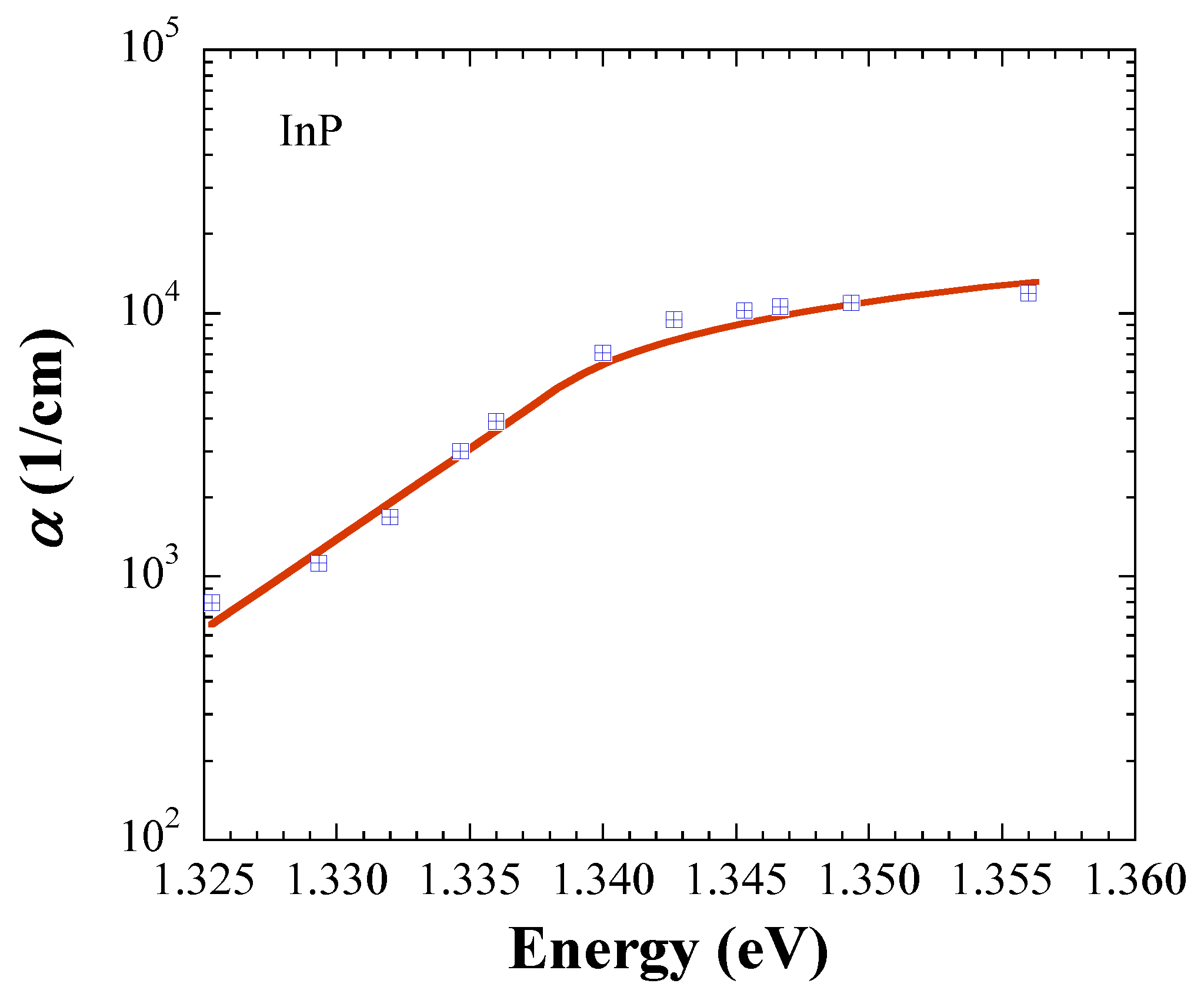
In this section, we demonstrate further evidence that the JDOS, which is defined with Equations (5) and (6), results in accurate Eg values. For this purpose, we retrieved absorption data at room temperature from the literature, and performed fits for crystalline InP [7], InAs [8], InSb [9], and GaAs [10]. The symbols in Figure 1, Figure 2, Figure 3 and Figure 4 represent the measurements, and the solid lines fits with Equations (5) and (6). All fits are carried out with kT = 0.025 eV, and Table 1 lists the fit parameters.
For comparison, Eg values from the literature are listed in Table 2 [11,12]. The fitted Eg values are in excellent agreement with the literature data for InP, InAs, and InSb, while the fit value of 1.416 ± 0.004 eV for GaAs is 0.014 eV below the numbers given in the literature, but coincides with 1.4287 ± 0.008 eV found by us in Ref. [6]. Table 3 shows α(Eg) calculated with the fit parameters in Table 1. Notably, the trend of the In-based semiconductors indicates that α(Eg) ∝ Eg, an observation, which justifies further investigation.
4. Discussion and Conclusions
While we used the JDOS represented by Equations (5) and (6) for II–VI and III–V compounds quite intensively over the years, among others, in Refs. [3,5,6,13,14,15], the model established popularity within the semiconductor society as well, i.e., other research groups used the model to fit the photoluminescence spectra of CdS nano-ribbons [16] and of InNAs alloys [17], and the absorption and photoconductivity of nanocrystalline bismuth (III) sulfide thin films [18], to refer to some of the appearances in the literature. Additionally, for comparison purposes to the band-fluctuations model in Ref. [1], the JDOS presented herein was used to fit α(E) and Eg of p-type bulk GaAs and nano-crystalline Ga1−xMnxN. Notably, referring to Figure 6a,c in Ref. [1], the fits with the band-fluctuation model and Equations (5) and (6) result in practically identical Eg values for both materials, reinforcing the correctness of our model.
We ought to mention that the only limitation for the presented model, in particular for Equation (1), we encountered when investigating the absorption of ZnS due to the material’s distinguished excitonic absorption, even at room temperature. Notably, however, since excitons do not contribute to photoconducting effects, Equations (5) and (6) describe the absorption transitions forming the photocurrent [15].
Concluding, the work emphasizes that the presented modified form of Urbach’s rule defines Eg, which, according to Equations (3) and (4), is located at the cross-over between the absorption regions reigned by DOS and band tails, respectively. The JDOS presented produces an explicit expression for α(Eg), and offers the experimental advantage of strong transmission signals from the highly transmissive spectrum of semiconductors to precisely determine the position of Eg.
Author Contributions
Conceptualization, B.U. and M.B.; methodology, B.U., M.B. and H.X.; validation, M.B., B.U. and H.X.; formal analysis, B.U., M.B. and H.X.; investigation, B.U., M.B. and H.X.; resources, M.B.; data curation, B.U. and M.B.; writing—original draft preparation, B.U., M.B. and H.X.; writing—reviewing and editing, B.U., M.B. and H.X.; visualization, M.B.; supervision, B.U.; project administration, M.B.; funding acquisition, M.B. All authors have read and agreed to the published version of the manuscript.
Funding
The research and the APC were funded by the professional development fund of Dr. Mithun Bhowmick.
Institutional Review Board Statement
Not applicable.
Informed Consent Statement
Not applicable.
Data Availability Statement
The data presented in this study are available on request from the corresponding author.
Conflicts of Interest
The authors declare no conflict of interest.
References
- Guerra, J.A.; Tejada, A.; Töfflinger, A.; Grieseler, R.; Korte, L. Band-fluctuations model for the fundamental absorption of crystalline and amorphous semiconductors: A dimensionless joint density of states analysis. J. Phys. D Appl. Phys. 2019, 52, 105303. [Google Scholar] [CrossRef]
- Pankove, J.I. Optical Processes in Semiconductors, 2nd ed.; Dover Publications: New York, NY, USA, 1971. [Google Scholar]
- Ullrich, B.; Singh, A.K.; Bhowmick, M.; Barik, P.; Ariza-Flores, D.; Xi, H.; Tomm, J.W. Photoluminescence lineshape of ZnO. AIP Adv. 2014, 4, 123001. [Google Scholar] [CrossRef] [Green Version]
- Urbach, F. The Long-Wavelength Edge of Photographic Sensitivity and of the Electronic Absorption of Solids. Phys. Rev. 1953, 92, 1324. [Google Scholar] [CrossRef]
- Ullrich, B.; Bouchenaki, C. Bistable Optical Thin CdS Film Devices: All-Optical and Optoelectronic Features. Jpn. J. Appl. Phys. 1991, 30, L1285. [Google Scholar] [CrossRef]
- Ullrich, B.; Singh, A.K.; Barik, P.; Xi, H.; Bhowmick, M. Inherent photoluminescence Stokes shift in GaAs. Opt. Lett. 2015, 40, 2580. [Google Scholar] [CrossRef] [PubMed] [Green Version]
- Turner, W.J.; Reese, W.E.; Pettit, G.D. Exciton Absorption and Emission in InP. Phys. Rev. 1964, 136, A1467. [Google Scholar] [CrossRef]
- Dixon, J.R.; Ellis, J.M. Optical Properties of n-Type Indium Arsenide in the Fundamental Absorption Edge Region. Phys. Rev. 1961, 123, 1560. [Google Scholar] [CrossRef]
- Moss, T.S.; Burrell, G.J.; Ellis, B. Semiconductor Opto-Electronics, 1st ed.; Wiley: New York, NY, USA, 1973. [Google Scholar]
- Moss, T.S.; Hawkins, T.D.F. Infrared absorption in gallium arsenide. Infrared Phys. 1961, 1, 111. [Google Scholar] [CrossRef]
- Bleicher, M. Halbleiter-Optoelektronik, 2nd ed.; Huethig: Heidelberg, Germany, 1985. [Google Scholar]
- Adachi, S. Properties of Group-IV, III-V and II-VI Semiconductors, 1st ed.; Wiley: Chichester, UK, 2005. [Google Scholar]
- Ullrich, B.; Yano, S.; Schroeder, R.; Sakai, H. Analysis of single- and two-photon-excited green emission spectra of thin-film cadmium sulfide. J. Appl. Phys. 2003, 93, 1914. [Google Scholar] [CrossRef]
- Ullrich, B.; Munshi, S.R.; Brown, G.J. Photoluminescence analysis of p-doped GaAs using the Roosbroeck Shockley relation. Semicond. Sci. Technol. 2007, 22, 1174. [Google Scholar] [CrossRef]
- Yano, S.; Schroder, R.; Ullrich, B.; Sakai, H. Absorption and photocurrent properties of thin ZnS films formed by pulsed-laser deposition on quartz. Thin Solid Films 2003, 423, 273. [Google Scholar] [CrossRef]
- Liu, D.; Pan, A.L.; Xu, G.; Bai, Y.; Zhu, X.; Zou, B.S. Self-Absorption Effect in the Spatial Resolved Spectra of CdS Nano-Ribbon Optical Waveguide Observed by Near-Field Spectroscopy. Opt. Rev. 2006, 13, 235. [Google Scholar] [CrossRef]
- Merrick, M.; Cripps, S.A.; Murdin, B.N.; Hosea, T.J.C.; Veal, T.D.; McConville, C.F.; Hopkinson, M. Photoluminescence of InNAs alloys: S-shaped temperature dependence and conduction-band nonparabolicity. Phys. Rev. B 2007, 76, 075209. [Google Scholar] [CrossRef] [Green Version]
- Pejova, B. Analysis of the shape of spectral dependence of absorption coefficient and stationary photoconductivity spectral response in nanocrystalline bismuth (III) sulfide thin films. Mater. Res. Bull. 2008, 43, 2887. [Google Scholar] [CrossRef]
Figure 1.
Absorption coefficient of InP. The symbols are retrieved from Ref. [7], and the solid line represents the fit with Equations (5) and (6).
Figure 1.
Absorption coefficient of InP. The symbols are retrieved from Ref. [7], and the solid line represents the fit with Equations (5) and (6).

Figure 2.
Absorption coefficient of InAs. The symbols are retrieved from Ref. [8], and the solid line represents the fit with Equations (5) and (6).
Figure 2.
Absorption coefficient of InAs. The symbols are retrieved from Ref. [8], and the solid line represents the fit with Equations (5) and (6).

Figure 3.
Absorption coefficient of InSb. The symbols are retrieved from Ref. [9], and the solid line represents the fit with Equations (5) and (6).
Figure 3.
Absorption coefficient of InSb. The symbols are retrieved from Ref. [9], and the solid line represents the fit with Equations (5) and (6).

Figure 4.
Absorption coefficient of GaAs. The symbols are retrieved from Ref. [10], and the solid line represents the fit with Equations (5) and (6).
Figure 4.
Absorption coefficient of GaAs. The symbols are retrieved from Ref. [10], and the solid line represents the fit with Equations (5) and (6).


| Bandgap Energy | InP | InAs | InSb | GaAs |
|---|---|---|---|---|
| A (eV−1/2cm−1) | 9 × 10⁴ ± 7560 | 1.9080 × 10⁴ ± 1488 | 8 × 10³ ± 416 | 3 × 10⁴ ± 3360 |
| σ | 3.96 ± 0.36 | 5.255 ± 0.851 | 4.885 ± 0.303 | 2.408 ± 0.130 |
| EgDOS (eV) | 1.335 ± 0.001 | 0.353 ± 0.002 | 0.173 ± 0.001 | 1.411 ± 0.003 |
| Eg (eV) | 1.338 ± 0.002 | 0.356 ± 0.003 | 0.176 ± 0.001 | 1.416 ± 0.004 |
| Bandgap Energy | InP | InAs | InSb | GaAs |
|---|---|---|---|---|
| Eg (eV) | 1.34 | 0.36 | 0.18 | 1.43 |
| Eg (eV) | 1.35 | 0.359 | 0.17 | 1.43 |
| - | α(Eg) (cm−1) |
|---|---|
| InP | 5057 ± 483 |
| InAs | 931 ± 105 |
| InSb | 405 ± 25 |
| GaAs | 2162 ± 249 |
Publisher’s Note: MDPI stays neutral with regard to jurisdictional claims in published maps and institutional affiliations. |
© 2021 by the authors. Licensee MDPI, Basel, Switzerland. This article is an open access article distributed under the terms and conditions of the Creative Commons Attribution (CC BY) license (http://creativecommons.org/licenses/by/4.0/).
Share and Cite
MDPI and ACS Style
Bhowmick, M.; Xi, H.; Ullrich, B. Optical Bandgap Definition via a Modified Form of Urbach’s Rule. Materials 2021, 14, 1639. https://doi.org/10.3390/ma14071639
AMA Style
Bhowmick M, Xi H, Ullrich B. Optical Bandgap Definition via a Modified Form of Urbach’s Rule. Materials. 2021; 14(7):1639. https://doi.org/10.3390/ma14071639
Chicago/Turabian StyleBhowmick, Mithun, Haowen Xi, and Bruno Ullrich. 2021. "Optical Bandgap Definition via a Modified Form of Urbach’s Rule" Materials 14, no. 7: 1639. https://doi.org/10.3390/ma14071639
Note that from the first issue of 2016, this journal uses article numbers instead of page numbers. See further details here.