

Abstract
GeSn alloys have emerged as promising materials for silicon-based optoelectronic devices. However, the epitaxy of pseudomorphic GeSn layers on a Ge buffer is susceptible to a significant compressive strain that significantly hinders the performance of GeSn-based photonic devices. Herein, we report on a new strategy to produce strain-free GeSn nanomembranes for advanced optoelectronic applications. The GeSn alloy was grown on a silicon-on-insulator substrate using Ge buffers, and it has a residual compressive strain. By transfer-printing the GeSn/Ge/Si multi-layers, followed by etching the Si template and the Ge buffer layers, respectively, the residual compressive strain was completely removed to achieve strain-free GeSn layers. A bandgap reduction was also observed as a result of strain relaxation. Furthermore, theoretical analysis was performed to evaluate the effect of strain relaxation on the GeSn-based optoelectronic devices. The proposed approach offers a practical and viable method for preparing strain-free GeSn alloys for advanced optoelectronic applications.
Export citation and abstract BibTeX RIS
1. Introduction
Group-IV germanium-tin (GeSn) material systems have recently gained increasing attention for optoelectronic applications [1, 2]. Pure Ge is a fairly abundant and less toxic semiconductor compared with III–V semiconductor compounds, and has been widely used in the current Si semiconductor electronics industry. However, the indirect bandgap of pure Ge prevents its applicability in high-performance optoelectronic applications. Fortunately, the energy difference between the direct conduction band and the lowest L-valley conduction band edge ( ) is only 136 meV at room temperature [3], thus suggesting the possibility of engineering the bandgap from indirect to direct to facilitate the use of the material in advanced optoelectronic applications. Extensive efforts have been made to enable indirect-to-direct bandgap transition. This indirect-to-direct bandgap transition can be achieved by alloying Ge with its group-IV neighbor, Sn [4]. The introduction of Sn into Ge significantly decreases both the direct and indirect bandgaps, resulting in reduced
  . With a Sn content of ∼6% [5], bulk GeSn can be transformed into a direct bandgap material, thereby making it suitable for efficient photonic devices. In addition, the bandgap energy of GeSn can be widely tuned by adjusting the Sn composition, thus offering a widely tunable range in the mid-infrared applications [6–8]. Although the solid solubility of Sn in Ge is less than 2% in equilibrium, recent advances in low-temperature (LT) growth techniques have enabled the growth of high-quality GeSn layers with a Sn composition up to 30% [6–13]. Based on this development, GeSn-based LEDs/lasers [9, 14–16], modulators [17], and photodetectors (PDs) [18–28] have also been recently demonstrated.
Although the GeSn material system exhibits great potential for optoelectronic applications, the epitaxial growth of GeSn experiences many challenges. The lattice constant of GeSn is more than 4.2% larger than that of Si, thus making it very challenging to directly grow high-quality GeSn layers on Si substrates. Instead, the Ge buffer technology was introduced to reduce the lattice mismatch between GeSn and the substrate [20, 21]. However, the disadvantage of the epitaxial growth of GeSn on the virtual Ge substrate is the introduction of a crucial compressive strain (∼0.143% per 1% Sn). As shown in figure 1, this compressive strain significantly impacts the band structure, this reducing the effect of Sn-alloying on the band structures, and thus, the performance of GeSn-based optoelectronic devices. The compressive strain can significantly increase both the direct and indirect bandgap energies. The direct bandgap energy shifts approximately five times faster than the indirect bandgap energy, thereby significantly increasing  [3]. As a result, the Sn content required to achieve indirect-to-direct bandgap transition is considerably increased from ∼6% for the bulk GeSn to ∼17% for the pseudomorphic GeSn on Ge [29]. This could significantly increase the level of challenge to achieve direct bandgap GeSn alloys. In addition, the compressive strain pushes the heavy-hole (HH) band above the light-hole (LH) band; thus the lowest direct bandgap is defined as the transition energy from the HH band to the Γ-conduction band. As a result, the increased direct bandgap due to the compressive strain will induce a blue shift in the direct-gap absorption edge [30], thereby counteracting the bandgap reduction by Sn-alloying and weakening the bandgap energy tunability for photonic devices. Furthermore, a higher Sn composition also degrades the thermal budget of GeSn alloys [31]. Therefore, it is crucial to relax the compressive strain in the GeSn films to enhance the performance of GeSn-based photonic devices.
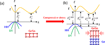
Figure 1. Schematic representation of the band structure of (a) strain-free and (b) compressively-strained GeSn alloys.
Download figure:
Standard image High-resolution imageTo address this challenge, several approaches have been developed to reduce the residual compressive strain in GeSn. For example, the use of III–V lattice-matched buffer layers for the growth of GeSn layers can effectively control the strain in the GeSn layer, and enhanced photoluminescence (PL) has been demonstrated [5]. However, because group-III and group-V materials are dopants for GeSn alloys, thus the auto-doping effect could significantly influence the optoelectronic properties of GeSn alloys and thus degrade the device performance. The growth of GeSn layers on graded GeSn buffers [9] can also relieve the compressive strain. However, the compressive strain usually cannot be fully removed. Lastly, GeSn suspending structures by selectively removing the Ge buffer layer [32] can also relax the compressive strain. However, the geometry and size are usually limited for device applications. In this paper, we present a new strategy to achieve strain-free GeSn alloys via a transfer-printing of nanomembranes (NMs), which does not have the above-mentioned limits. Single-crystalline semiconductor NMs are transferrable free-standing thin films with unique advantages such as excellent mechanical flexibility and material quality (e.g. high mobility and light absorption, and scalable size), and transfer-printing technique has been utilized to fabricate Ge and III–V NMs [33–39]. By transfer-printing the GeSn NMs and carefully removing the Ge buffer layer, the compressive strain that was initially stored in the GeSn was successfully removed. The structural properties of transfer-printed GeSn NMs were systematically investigated using x-ray diffraction (XRD) and Raman spectroscopy. Furthermore, the bandgap variation due to the strain relaxation was confirmed based on transmission and PL experiments. The impact of strain relaxation on the bandgap energy of GeSn was theoretically analyzed. These results demonstrate a practical method for achieving strain-free GeSn layers for advanced optoelectronic applications.
2. Results and discussion
The sample used in this study was grown using solid-source molecular beam epitaxy (MBE) on a (001) silicon-on-insulator substrate (SOI) substrate with a 2.5 μm thick top Si layer and a 1 μm thick buried oxide (BOX) layer. Here, the BOX layer functions as the sacrificing layer for the undercut process. A 120 nm thick Ge virtual substrate was initially grown using a two-step growth technique, consisting of a 60 nm Ge buffer layer grown at a LT of 350 °C, followed by an in-situ annealing at 800 °C for 5 min. A 60 nm Ge buffer layer was further grown at a high temperature (HT) of 550 °C. Subsequently, the growth temperature was decreased to 150 °C to facilitate the growth of a 370 nm thick GeSn layer. Finally, a 3nm thick Si cap layer was deposited. The structural properties and Sn composition of the grown GeSn sample were systematically investigated using secondary ion mass spectroscopy (SIMS) and XRD. Figure 2(a) shows the SIMS atomic distributions of the Ge and Sn atoms along the growth direction, from which the thickness of the GeSn layer is determined to be 370 nm. A uniform Sn distribution was confirmed in the GeSn layer. Figure 2(b) shows the XRD (224) reciprocal space mapping (XRDRSM) results for the grown GeSn sample. Several peaks were observed, which are associated with the LT Ge buffer, HT Ge buffer and GeSn layers, respectively. From the results, a compressive strain of 0.48% was found in the LT Ge buffer layer due to the lattice mismatch between Si and Ge to promote an intermediate islanding process and confine misfit dislocations. The GeSn peak and HT Ge peak were aligned at the Qx, as indicated by the pseudomorphic line, thereby suggesting that the GeSn layer was pseudomorphic with respect to the HT Ge buffer layer. From the Qx value, the in-plane lattice constant was obtained as  = 5.6616 Å, which is slightly larger than that of bulk Ge (
 = 5.6573 Å [40]), suggesting an in-plane strain of 0.077% in the HT Ge buffer due to the difference between thermal expansion coefficient of Si and Ge [27]. On the other hand, from the Qy value of the GeSn peak, the out-of-plane lattice constant of GeSn was obtained as
  = 5.6989 Å. With the in-plane and out-of-plane lattice constants, the bulk lattice constant of the GeSn layer can be obtained using [21, 31]:
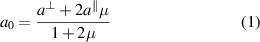
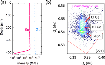
Figure 2. (a) SIMS depth profile along the growth direction and (b) (224) x-ray reciprocal space mapping of the grown GeSn sample.
Download figure:
Standard image High-resolution imagewhere  is the ratio of the elastic constants and the value for Ge1−xSnx is
  [7]. On the other hand, the composition-dependent lattice constant of bulk Ge1−xSnx is:

where  = 5.6573 Å and
  = 6.4892 Å are the bulk lattice constants of Ge and α-Sn, respectively, and
  Å is the bowing parameter [7]. Substituting the extracted lattice constant of GeSn from the XRDRSM experiments into equation (2) yields
  = 3.3% for the grown GeSn sample. The corresponding in-plane biaxial strain in the GeSn layer is
  .
.
Figure 3 depicts a schematic representation of the process used to obtain strain-free GeSn NMs. In short, the strain-free GeSn NMs were fabricated using a transfer-printing technique, followed by the removal of the Ge buffer layer. The process began with the epitaxial growth of the 370 nm GeSn alloy using MBE (figure 3(a-i)). Standard photolithography and dry etching were used to pattern the NMs with an array of etching holes having a diameter of 3 μm and a period of 50 μm, followed by a hydrofluoric (HF) undercut process (figure 3(a-ii)) [32]. Then, the released NMs (i.e. GeSn/Ge/Si) were flip transfer-printed on an adhesive layer (SU-8 2002) with a thickness of ∼2 µm, then coated on the 120 µm polyethylene terephthalate (PET) (figure 3(a-iii)). Figure 3(b) depicts the corresponding cross-sectional structure of NMs in the respective steps. The printed NMs had a Si template layer facing the top (figure 3(b-iii)). Finally, the strain-free GeSn NMs with a final thickness of ∼200 nm were obtained by a precise CF4 gas-based etching of the top Si template and Ge buffer layers, respectively (figure 3(a-iv)). In addition, the change in surface roughness was measured by atomic force microscopy (AFM). As shown in figure 3(c), the root mean square (RMS) roughness of GeSn on the SOI is 6.24 nm. The flip-transferred GeSn NMs had an RMS roughness of 1.46 nm with the Si template layer positioned face up. It is widely known that a smooth interface exists between the Si template and the BOX layers of the SOIs fabricated using a Smart-Cut technique [41]. A final RMS roughness of 3.6 nm was measured from the strain-free GeSn NMs. The result indicates that the surface roughness of the GeSn was reduced, which enables further device fabrication. In addition, although the RMS value seems larger than that of polished surfaces and surface defects could be created as recombination sites, proper surface passivation via atomic layer deposition can minimize recombination to maintain good device performance [42]. In addition, this level of nano-roughened surface can be effective to modulate Schottky barrier height, leading to suppressed background signal [43].
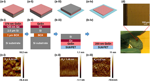
Figure 3. (a) The schematic representation of the fabrication of strain-free GeSn NMs; (a-i) Growth of a 370 nm thick GeSn alloy on a SOI substrate by MBE, (a-ii) Patterning NMs with an array of etching holes followed by an HF undercut process, (a-iii) Flip-transferring of 3 × 3 mm2 sized GeSn NMs on SU-8 2002 coated PET substrates, with the Si template layer facing the top, (a-iv) Preparation of strain-free GeSn NMs via etching down to the GeSn layer by removing the top Si template and Ge buffer layers. (b) and (c) Corresponding cross-sectional view and AFM images for each step. (d) An optical image of strain-free GeSn NMs on PET and its magnified microscopic image.
Download figure:
Standard image High-resolution imageTo examine the strain relaxation of the transfer-printed GeSn layer, XRD and μ-Raman spectroscopy were conducted. Figure 4(a) shows the x-ray 2θ scans for the as-grown GeSn sample, the transfer-printed GeSn NMs, and a bulk Ge wafer. From the Bragg angle (θ), the out-of-plane lattice constant can be determined via  , where
  is the wavelength of the x-ray. The Bragg angle of the as-grown GeSn sample was noticeably smaller than that of bulk Ge because of the larger lattice constant of GeSn and the out-of-plane tensile strain. In addition, the Bragg angle of the transfer-printed GeSn NMs is significantly larger than that of as-grown GeSn sample, thus highlighting the significant strain relaxation. From the Bragg angle, the out-of-plane lattice constant of the transfer-printed GeSn is extracted as
  5.686 Å. This value is almost identical to the bulk lattice constant of the GeSn layer (a0 = 5.685 Å), thereby suggesting that the transfer-printed GeSn layer is strain-free. These results demonstrate that the compressive strain stored in the GeSn layer can be removed using the transfer-printing techniques. It is also noted that the full-width-at-half-maximum (FWHM) of the GeSn peak for the transfer-printed GeSn NMs becomes broader than that of the as-grown GeSn sample, which may be attributed to the uniformity and surface roughness of the transfer-printed GeSn films.

Figure 4. (a) 2θ scans and (b) Raman spectra for the as-grown GeSn sample, transfer-printed GeSn sample, and bulk Ge.
Download figure:
Standard image High-resolution imageThe μ-Raman experiments were conducted under a backscattering scheme with an unpolarized 633 nm laser focused onto the sample surface via a 20× objective with a spot size of ∼10 μm, in which the LO phonon mode was obtained. The intensity of the laser was intentionally kept low to hinder the thermal heating effect. Figure 4(b) shows the Raman shifts for bulk Ge, as-grown GeSn, and transfer-printed GeSn measured at room temperature. A peak was observed at 300 cm−1 for bulk Ge, which is associated with the Ge-Ge LO phonon mode. For the as-grown GeSn sample, the Raman peak shifted to a lower wavenumber compared with the bulk Ge reference because of the introduction of Sn. The main peak associated with a shoulder at a higher wavenumber was observed. The former and latter peaks are attributed to the Ge-Ge LO phonon mode from the GeSn and the Ge buffer layers, respectively. The peak values were obtained by fitting the data using Gaussian functions, and the results were displayed as the solid lines in figure 4(b), yielding  for the GeSn layer. For transfer-printed GeSn NMs, it is evident that the Raman peak shifted further to a lower wavenumber of
  , which again supports the strain relaxation in GeSn NMs. For biaxially stressed Ge1−xSnx layers, the Raman shifts of the Ge-Ge LO mode can be linked to the Sn composition and the in-plane strain by [32]:

From the Sn composition and strain values obtained from the x-ray experiments and the Raman shifts, we obtained  and
and  , which are in good agreement with recent works [32].
To confirm the bandgap variation caused by strain relaxation, transmission experiments at room temperature were performed using micro-Fourier transform infrared microscopy in a normal incidence transmission configuration with a spot size of ∼10μm.
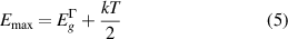
Figure 5(a) depicts the measured absorbance spectra of the as-grown GeSn on SOI and transfer-printed GeSn NMs. For the as-grown GeSn on SOI, the absorbance spectrum exhibits significant ripple structures because of the vertical cavity created by the top GeSn/air interface and the bottom BOX/Si interface that cause significant interference in the layers [15]. The absorbance reduces at a photon energy of ∼700 meV, corresponding to the direct-gap absorption edge of the pseudomorphic GeSn layer. On the other hand, for the transfer-printed GeSn NMs, less significant ripple structures in the spectral region were observed. The comparison of the absorbance spectra reveals the differences in the layer structures. To extract the direct bandgap, the Tauc equation was employed [7]:

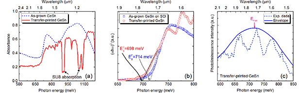
Figure 5. (a) Measured absorbance spectra of the as-grown GeSn sample and transfer-printed GeSn nanomembrane. The signal distortions near 1200 and 1400 nm are attributed to the absorption by the SU8 layer. (b) Tauc plots of the as-grown GeSn sample and transfer-printed GeSn nanomembrane for the determination of direct bandgap. The dashed line represents the linear fit near the band edge. (c) Measured room-temperature photoluminescence (PL) spectrum from the transfer-printed GeSn sample. The solid line shows the envelop of the PL spectrum and the envelop maximum is indicated by the red arrow.
Download figure:
Standard image High-resolution imagewhere  is the absorption coefficient, A is an energy-independent constant, and
  is the photon energy. Figure 5(b) depicts the Tauc plot that was converted from the absorbance spectra for the as-grown GeSn on the SOI and the transfer-printed GeSn NMs. Fitting the Tauc plot near the band edge using equation (4) yields a direct bandgap
  and
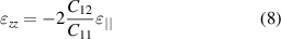
and  for the as-grown GeSn on SOI sample and the transfer-printed GeSn NMs, respectively. The observed reduction in the direct bandgap is attributed to the strain relaxation in the GeSn NMs. To further confirm the direct bandgap energy of the transfer-printed GeSn NMs, PL experiments was conducted at room temperature using a 532 nm laser as the light source. The laser intensity was intentionally kept low to hinder the thermal heating effect. The measured PL spectrum for the transfer-printed GeSn NMs is depicted in figure 5(c). Several emission peaks were observed due to the interference in the GeSn NMs. To obtain the emission peak, the envelop of the PL spectrum was extracted, as shown in figure 5(c), where the envelop maximum (
 ) is indicated by the red arrow.
  is related to the direct bandgap energy by [44]
where k is the Boltzmann constant and T is the temperature. Using the value of  obtained from the PL spectrum and equation (5), we obtain
  for the transfer-printed GeSn NMs, which is in good agreement with the results from transmission experiments. To further confirm the bandgap reduction by the strain relaxation effect, we analyzed the strained bandgap energy using deformation potential theory [30, 40]. The direct bandgap of pseudomorphic Ge0.0967Sn0.033 on the Ge buffer and the strain-free Ge0.0967Sn0.033 NMs are calculated to be 708 meV and 683 meV, respectively, which are in good agreement with the experimental results.
Having demonstrated the achievement of strain relaxation using transfer-printing techniques, we theoretically discuss the impact of strain relaxation on the bandgap energies of GeSn alloys for advanced optoelectronic applications. In the case of the GeSn layers pseudomorphically grown on Ge buffer layers (figure 1(b)), the layers are subjected to an in-plane biaxial compressive stress, which significantly impacts the band structure. First, the compressive strain pushes both the Γ- and L-conduction band edges up. In addition, it splits the degeneracy of the valence band and brings the HH band above the LH band. As a result, the top valence band is HH-like, and the lowest direct (indirect) bandgap is defined as the energy difference between the Γ-valley (L-valley) conduction band and the HH band,  (
( ). We then calculate the strained band structures. For strain-free Ge1−xSnx alloys, the band gap energies can be expressed as [40]

where η represents the different valleys,  and
and  are the bandgap energies of Ge and α-Sn, respectively, and
  is the bowing parameter. The values used in these calculations are given in table 1.
Table 1. Bandgap parameters for GeSn [5, 40].
 (eV) (eV) |  (eV) (eV) |  (eV) (eV) | |
|---|---|---|---|
| Γ-valley | 0.7985 | −0.413 | 2.42 |
| L-valley | 0.664 | 0.092 | 0.89 |
For Ge1−xSnx alloys grown along the  direction subjected to a biaxial stress along
  and
and  direction, the strain fields can be expressed as:


The dispersion relationship for the electrons in the Г-conduction band ( ) and the L-conduction band (
 ) as well as for the holes in the valence band
  , with m being HH or LH, can be calculated using a multi-band
  method taking into account the effects of the strain and band nonparabolicity [30, 45]. After the strained band structures are calculated, we calculated the optical absorption coefficient and light-emission efficiency for strain-free and compressively GeSn alloys. The direct-gap optical absorption coefficient can be calculated using Fermi's golden rule as follows [30]
where  is the refractive index, c is the velocity of light in free space, e is the electronic charge, ħ is the reduced Planck's constant, m0 is the mass of free electrons, ε0 represents the free-space permittivity, ω is the angular frequency of incident light,
  is the momentum matrix, with
  being the photon energy, and γ is the FWHM of the Lorentzian lineshape. The value of γ used in this study is 15 meV. On the other hand, the spontaneous emission rate per unit volume per unit energy interval (rsp) can be calculated using [45]
where  and
and  are the Fermi–Dirac distribution for electrons in the conduction band and valence band, respectively. The parameters used in this calculation are obtained from the linear interpolation between Ge and α-Sn, which can be found in [40].
Figure 6(a) shows the calculated  for the biaxially stressed Ge1−xSnx alloys in terms of the Sn composition and the in-plane strain, in which the pseudomorphic Ge1−xSnx on Ge is indicated by the white dashed line. As the Sn content increases, the resultant compressive strain also increases, thereby significantly increasing the
  and redshifting the absorption edge. This property is crucial for PD applications when the GeSn is used as the active layer. Figure 6(b) depicts the comparison of the calculated absorption coefficient spectra for the pseudomorphic Ge1−xSnx on Ge and the strain-free Ge1−xSnx. The pseudomorphic Ge1−xSnx on Ge exhibits a larger
  and thus, a shorter cutoff wavelength and smaller absorption coefficient than the strain-free Ge1−xSnx. As a result, PDs with a pseudomorphic Ge1−xSnx on Ge as the active layer exhibit a weaker quantum efficiency and narrower photodetection range than the counterparts with strain-free Ge1−xSnx active layer. Thus, it is critically important to relax the compressive strain to enhance the performance of GeSn-based PDs. Second, the compressive strain also significantly impacts the light-emitting efficiency of GeSn. Figure 6(c) shows the calculated
  for the biaxially stressed Ge1−xSnx alloys as a function of Sn composition and in-plane strain, where the pseudomorphic Ge1−xSnx on Ge is represented by the white dashed line. The introduction of Sn significantly reduces the
  to achieve an indirect-to-direct bandgap transition. For the strain-free GeSn alloys, our calculations demonstrate that a Sn content of 6.6% is sufficient to achieve the direct bandgap. As a result, the GeSn alloys can be used as efficient light emitters. However, the compressive strain hinders the reduction of
  by Sn-alloying. As a result, a much higher Sn content of 16.01% is required to achieve the indirect-to-direct bandgap transition, which agree with the results reported in [29] and [46]. The slight discrepancy may arise from the parameters used in the calculation, and a more accurate prediction is possible when more reliable material parameters are available. Hence, fewer electrons will be injected into the direct conduction band for efficient electron-hole recombination in the case of the pseudomorphic Ge1−xSnx on Ge, compared with that of the strain-free Ge1−xSnx. To highlight the effect of the compressive strain, figure 6(d) shows the comparison of the calculated rsp for the pseudomorphic Ge1−xSnx on Ge and that of the strain-free Ge1−xSnx. As the Sn content increases, the rsp significantly increases due to the reduced
  . However, the pseudomorphic Ge1−xSnx on Ge exhibits a much weaker rsp than the strain-free Ge1−xSnx due to the larger
  . The presence of compressive strain can significantly reduce the light-emitting efficiency of the GeSn light emitters, thereby increasing the threshold of GeSn lasers. This analysis highlights the importance of relaxing the compressive strain stored in the GeSn layers for optoelectronic applications. Therefore, our proposed transfer-printing technique can provide a viable approach for achieving high-performance GeSn optoelectronic devices.


Figure 6. (a) Calculated lowest direct bandgap energy ( ) of Ge1−xSnx alloys as a function of in-plane compressive strain and Sn composition. (b) Calculated absorption coefficient spectra of pseudomorphic Ge1−xSnx on Ge and strain-free Ge1−xSnx with different Sn compositions. (c) Calculated energy difference between the direct and indirect conduction bands (ΔEΓL) of Ge1−xSnx alloys as a function of in-plane compressive strain and Sn composition. (d) Calculated spontaneous emission rate per unit volume per unit energy interval for pseudomorphic Ge1−xSnx on Ge and strain-free Ge1−xSnx with different Sn compositions.
Download figure:
Standard image High-resolution image
While the strain-free GeSn NMs were obtained from the GeSn films grown on a SOI substrate, it is also possible to forms releasable GeSn NMs on Si substrate without sacrificial layers. One feasible approach is to exploit large differences in wet chemical etching of the underlying Si substrates along planes of Si(110) and Si(111) using boiled potassium hydroxide (KOH) [47]. However, the size of releasable GeSn NMs will be strongly limited by lateral etching distance of Si(110) planes. In addition, good protection layers will be required to obtain damage-free GeSn NMs. Furthermore, compared with Ge or III–V NMs, it is more challenging to prepare strain-free GeSn NMs because the Ge buffer layer has to be properly removed for relaxing the strain. In addition, the increase of Sn content can lead to an increased defect density and a lower thermal budget. Further optimization of the fabrication will be necessary to prepare high-quality strain-free GeSn NMs for advanced optoelectronic applications.
3. Conclusions
In conclusion, we have developed a novel approach to achieve strain-free GeSn NMs for advanced optoelectronic applications. Pseudomorphic GeSn alloys with a Sn composition of 3.3% were first grown on SOI substrates via a Ge buffer using MBE. A significant amount of compressive strain was induced in the GeSn alloys due to the Ge buffer layer, which was completely removed by the transfer-printing of GeSn/Ge/Si multi-layers followed by the removal of the Si template and the Ge buffer layer, supported by the structural analysis. The reduction of the direct bandgap energy of GeSn from 714 to 698 meV was experimentally confirmed by transmission experiments. The effect of compressive strain on the bandgap energies, absorption coefficient, and light-emitting efficiency was theoretically studied, highlighting that the relaxation of compressive strain can significantly enhance the performance of GeSn PDs and light emitters. Overall, our novel approach for fabricating the strain-free GeSn NMs provides a great potential for high-performance GeSn optoelectronic device applications.
Acknowledgments
This work at CCU was supported by the Ministry of Science and Technology of Taiwan (MOST) under the Grant Nos. MOST 108-2221-E-194-055 and MOST 109-2636-E-194-002, and the Advanced Institute of Manufacturing with High-tech Innovations (AIM-HI) from The Featured Areas Research Center Program within the framework of the Higher Education Sprout Project by the Ministry of Education (MOE) in Taiwan. The work at Nanyang Technological University was supported by NTU start-up grant (M4082289.040) and Singapore MOE AcRF Tier 1 grant (M4012124.040). The authors would like to thank Dr Hui Li at National Taiwan University, Taiwan, for providing assistance in the material growth, and Dr I-Fang Cheng at Taiwan Semiconductor Research Institute (TSRI), Taiwan, for providing assistance in the Raman experiments.