
Abstract
The optical properties of zinc oxide (ZnO) nanorods (NRs) synthesized by the low-temperature aqueous chemical method on top of silicon (Si) substrate have been investigated by means of photoelectron energy loss spectroscopy (PEELS). The ZnO NRs were obtained by the low temperature aqueous chemical synthesis on top of Si substrate. The measured valence band, the dynamical dielectric functions and optical absorption of the material show a reasonable agreement when the trending and shape of the theoretical calculations are considered. A first-principle calculation based on density functional theory (DFT) was performed using the partially self-consistent GW approximation (scGW0) and compared to the experimental results. The application of these two techniques brings a new analysis of the electronic properties of this material. The experimental results regarding the density of states (DOS) obtained for the valence band using x-ray photoelectron spectroscopy (XPS) was found to be consistent with the theoretical calculated value. Due to this consistency, the same wavefunctions was then employed to calculate the dielectric function of the ZnO NRs. The experimentally extracted dielectric function was also consistent with the calculated values.
Export citation and abstract BibTeX RIS

Original content from this work may be used under the terms of the Creative Commons Attribution 3.0 licence. Any further distribution of this work must maintain attribution to the author(s) and the title of the work, journal citation and DOI.
1. Introduction
Possessing unique optical, electronic and piezoelectric properties especially into its nanostructured form, zinc oxide (ZnO) is considered as one of the most promising semiconductor materials for many applications [1–5]. In particular, ZnO nanorods (NRs) possess an excellent optical properties such as direct wide bandgap (3.7 meV, at room temperature) together with relatively high exciton binding energy (60 m eV) and the presence of the light emitting intrinsic point defects [1–4]. All these optical properties makes ZnO NRs to have a potential in the development of many functional devices such as ultraviolet (UV) photodetectors [6–8], light-emitting diodes (LEDs) [9–12] and solar cells [13]. However, the potential of ZnO NRs in all these applications would require a deep investigation of their optical properties [1–5]. To investigate these optical properties in more details and to fulfill the advantage of ZnO NRs in all the above mentioned applications a non-conventional characterization technique has been used.
That optical analysis is veryimportant for investigate the electronic properties of that semiconductor, but it is quite limited into a small energy range (up to 5 eV) rather considering onlydirect transitions, i.e., with no momentum transfer. Nevertheless, the electronic properties in solidsoften involve the transitions of states out of equilibrium regime by the occupation of excited states. This kind of transitions roles on the inelastic process those are responsible for the absorption of the material—therefore acting on the gap—at upper energy ranges that cannot be computed by optical techniques.
The PEELS technique was applied to the sample of ZnO NRs from its XPS spectratoevaluate the electronic properties by retrieving the experimental dielectric function [14, 15]. This technique has the advantage to extendenergy range of analysis towards higher energies, where we cannot have access by optical techniques. Therein, we probe the response of the material toelucidating the electronic dynamics at that region to explain the electronic properties of the NRs.
In order to have a theoretical framework of the electronic properties of the ZnONRs, we alsoperformed ab-initio calculations that allow us to make an integrated analysis—experiment and theory. The DFT was used by the ScGW method to evaluate the density of states (DOS) dielectric functionand absorption for ZnO,
The PEELS technique has been revealed as an important technique to retrieve the dielectric function of a material. It is a non-destructive method to obtain the dielectric function of the material from XPS spectra; it carries the sensitivity of the surface that is quite useful for the characterization of surfaces at nano-scale.
The PEELS technique consistsof the determination of the dielectric function ε(ω) based on the energy loss function (ELF) on XPS. Thisfunction contains the inelastic process that is related with ![$\text{Im}\left[-\tfrac{1}{\varepsilon }\right],$](https://content.cld.iop.org/journals/0268-1242/34/4/045019/revision2/sstab0bc4ieqn1.gif) according to the validity of the classical electromagnetic theory.
according to the validity of the classical electromagnetic theory.
2. Sample preparation
ZnO NRs under investigation were synthesized by the low-temperature aqueous chemical method on n-type silicon substrate. In brief, a 0.075 M synthesis solution was prepared by dissolving hexamethylenetetramine (HMTA) and zinc nitrate hexahydrate in deionized (DI) water and then stirred for 5 h at room temperature. After that, n-type silicon substrates pre-coated with ZnO nanoparticles (NPs) seed layer solution (prepared with zinc acetate, potassium hydroxide (KOH) having a molar ratio of 1:5) were submerged horizontally inside the synthesize solutions and kept in a preheated oven at 90 °C for 5 h. Afterward, the samples were carefully rinsed with DI-water to remove any residuals and finally, dried using blowing nitrogen. The synthesis process of the ZnO NRs and the preparation of the ZnO NPs seed layer solutions are described in more details in [12, 13, 16, 17].
The morphology of the synthesized ZnO NRs was characterized using field-emission scanning electron microscopy (FE-SEM) (Gemini LEO 1550). The optical properties were investigated by photoelectron energy-loss spectroscopy and first-principles calculation based on density functional theory (DFT).
3. Getting the sample dielectric function by photoelectron energy-loss spectroscopy (PEELS)
X-Photoelectron Spectroscopy was used to determine the dielectric function of the ZnO NRs sample. It is well-known that high-energy electrons crossing the material interact with the valence and free electrons in the material, exciting plasmon collective oscillation modes and losing kinetic energy [18–20]. It was demonstrated that this effect is related to the imaginary part of the inverse of the dielectric function of the material [21]. This property was initially used to determine the dielectric function of materials in EELS [22]. The deconvolution of multiple plasmon energy-loss spectra obtained by XPS was treated by Tougaard [23, 24]. The angular dependence of the plasmon energy-loss intensity in XPS spectra was studied by Werner [25]. This theoretical background was applied to determine dielectric functions of amorphous materials and crystalline oxides [14, 26–28]. Recently, a more accurate method was introduced to separate the elastic peak and the energy-loss spectrum, based on the Fourier transform of the XPS spectrum [15, 29], and it was applied to these ZnO NRs samples.
4. Computational methodology
In order to get a lattice parameter closer to experimental, the 4 atoms cell was relaxed using the AM05 functional [30, 31], giving the lattice parameters a = 3.241 and c = 5.237. AM05 is a function based on the Airy electron gas together with the uniform electron gas, where different regions have different approximations for the exchange-correlation potential based on the density and parameters obtained through a fit to the jellium energy data. The main calculation was performed using the partially self-consistent GW approximation (scGW0) [32], where only the Greens function was updated. This gives a good band gap of Eg = 3.32 eV. The GW was done using an 8 × 8 × 8 k-mesh with ∼110 empty bands. A cutoff energy of 400 and 300 eV was used for the GGA and GW parts, respectively. All the calculations were performed using VASP [33, 34] together with the linear response theory [35] to obtain the dielectric function.
5. Results and discussions
Below the different obtained results are presented and discussed.
5.1. Scanning electron microscopy analysis
Figure 1 shows a top-view field-emission scanning electron microscopy (FE-SEM) image of the synthesized ZnO NRs grown on silicon substrate. As can see from the FE-SEM image the NRs are highly dense and exhibit the hexagonal structure of ZnO. In addition, the NRs are slightly vertically aligned on the substratebut favor the observation of surface Plasmon. The detection area is about some square mm and the measurement is an average over this structure.

Figure 1. Top-view FE-SEM image of the ZnO NRs grown on Si substrate.
Download figure:
Standard image High-resolution image5.2. Plasmons, dielectric functions and absorption measurements
XPS spectra of the ZnO NRs samples were obtained with a SPECS Phoibos 100 1D-DLD spectrometer. The x-ray source was a non-monochromatic Mg Kα (1253.6 eV) operating at 130 W. Survey spectrum was registered with pass energy of 30 eV. Pass energy of 16 eV and of 30 eV were used for the valence band and for the O1s spectra, respectively. Figure 2 shows the XPS survey spectrum of the #515 sample (which prepared from synthesis solution stirred for 5 h and grown on ZnO seed prepared from zinc acetate, potassium hydroxide (KOH) having a molar ratio of 1:5). The principal elastic lines and their corresponding energy-loss spectra that could be analyzed to get the dielectric function of the material are indicated. Despite the facts that it corresponds to a doublet and that the energy range is limited to 70–130 eV region, the Zn 3p energy-loss spectrum is more favorable than the Zn 3d line that is mixed to the valence band, the Zn 3s that has a small intensity, or the O 1s line which is a complex line because of several different chemical binding. The Fourier method is able to analyze a doublet, particularly if the widths of the two lines are very similar. For the x-ray source, a multiline description with four mains lines was adopted as shown in table 1:
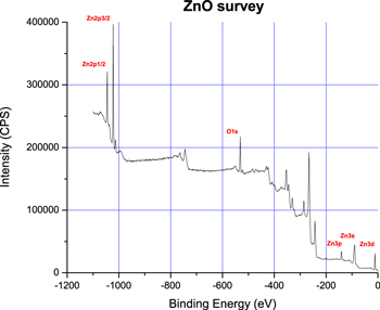
Figure 2. XPS survey spectrum of the synthesized ZnO NRs (LAS-IQ-UFBA—2018).
Download figure:
Standard image High-resolution imageTable 1. Position, intensity and width of the four lines considered to describe the multiline characteristic of the Mg Kα x-ray source.
| (i = 1 to 4) | Main | Satellite 1 | Satellite 2 | Satellite3 |
|---|---|---|---|---|
| Position (eV) Ei | 0.00 | 4.66 | 8.39 | 10.16 |
| Amplitude Ai | 1.0 | 0.010 | 0.063 | 0.037 |
| Width (eV) γi | 0.3 | 1.0 | 0.4 | 0.5 |
The profile of each line of the Zn 3p doublet was modeled by the Wertheim and Citrin theory [36], choosing the following parameters given in table 2 below:
Table 2. Parameters used in the Wertheim and Citrin model to describe the Zn 3p doublet line profile.
| Parameter | Value |
|---|---|
| Case | N(E) constant with a gap at EF |
| Fermi energy EF | 10.0 eV |
| Gap energy EG | 3.2 eV |
| Lorenztian width γ | 0.75 eV |
| Asymmetric coefficient α | 0.125 |
| spin–orbit gap ΔSO | 2.9 eV |
| 3p1/2/3p3/2 ratio | 0.51 |
The enlargement due to the spectrometer, and secondarily to the phonons, is supposed to be Gaussian with σ = 1.0 eV.
With these parameters it was possible to adjust the doublet to the XPS spectrum and derive the energy-loss function using the formula, in the Fourier transform spectrum [XPS_13]:
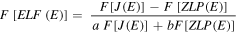
Where F[J(E)] is the Fourier transform of J(E), the XPS spectrum, F[ZLP(E)] is the Fourier transform of ZLP(E), the zero-loss peak, and a and b the Hüfner coefficients, taken equal to: a = 0.8 and b = 0.2. The Fourier spectrum was filtered with Hanning filter reducing the Fourier range to 1/4 of the full window. Small negative values near the elastic peek (E < 2 eV) were suppressed. The result of this treatment is presented in figure 3.

Figure 3. Plasmon extraction.
Download figure:
Standard image High-resolution imageAn energy gap of 3.2 eV was observed and the plasmon peak close 108 eV, before the energy-loss spectrum maximum because the enlargement due to the doublet was suppressed.
After this step, the Kramers-Krönig analysis is applied to obtain the dielectric function of the material (as shown figure 4), the inelastic mean free path (IMFP) and compute the Bethe sums giving the number of electrons involved in the plasmon [22]. The parameters used for this analysis are the index of refraction at E ≈ 0, n(0) = 2, the critical scattering angle, θc = 70 mrd, the surface plasmon amplitude, SEP =0.15, and the atomic density, Na = 4.15 × 1028 m−3.
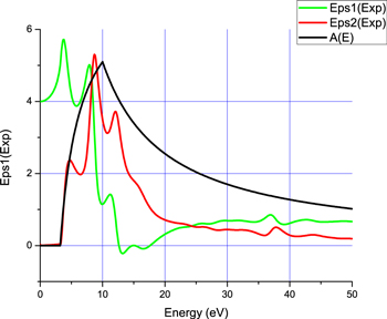
Figure 4. Real and imaginary parts of the Dielectric function, and joint-DOS function of the Wertheim and Citrin model.
Download figure:
Standard image High-resolution imageThe Wertheim and Citrin joint-DOS function A(E) was verified to be coherent with the obtained ε2(ω) function, exhibiting a gap of 3.2 eV. The IMFP is found close to 1.9 nm and the number of effective electrons larger than 9, which is coherent with the number of electron in the ZnO valence band.
The experimental dielectric functions obtained from PEELS were compared to theoretical results obtained by DFT with the GW method (figure 5). Globally, the experimental and the theoretical functions are very similar. However, it can be seen that the main absorption peak is translated to a lower energy.
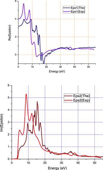
Figure 5. Comparison of experimental and theoretical dielectric functions.
Download figure:
Standard image High-resolution image5.3. Valence band spectrum
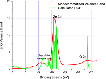
We also measured the valence band spectrum of the #515 sample (as shown in figure 6). As the X-source is multiline, the valence band spectrum was monochromatized. If we compare it to the theoretical DOS, we observe that the overall behavior is similar, but it seems that states are present in the forbiddenband.
Figure 6. Comparison of experimental XPS valence band x calculated DOS. We notice a good agreement between the Zn 3d and O 2s subshells with the photoemission spectra.
Download figure:
Standard image High-resolution image
5.4. Resistivity
In order to verify the presence of states near the minimum of the conduction band, we measure using a four-point method the resistance of our samples. Table 3 shows the resistance of the synthesized ZnO NRs grown from synthesis solution stirred at different durations such 3, 5 and 15 h and ZnO seed layer prepared with different molar ratios such as 1:1, 1:5 and 1:5 respectively.
Table 3. Resistance of several samples by the four-point method with d = 4 mm.
| Sample | R (MΩ) |
|---|---|
| #315 | 0.80 |
| #515 | 0.16 |
| #1511 | 0.80 |
| #1513 | 0.80 |
| #1515 | 0.20 |
The values obtained appear to be high, but it can be seen from the SEM images that, due to the morphology of the film, the conduction takes place through the possible contacts between NRs. There is no conduction through the substrate which is an intrinsic Si plate. With this simple model in mind, we determine a rough value of the ZnO NRs resistivity using the formula:

Where R is the measured resistance, ρ the resistivity, d the distance between the measurement points and w the width of each facet of the NRs. We find ρ varying between 1.5 × 10⁻⁴ to 6.0 × 10⁻⁴ Ω.cm, about one hundred times the resistivity of copper or tungsten.
6. Conclusion
We investigated the optical properties of ZnO nanorods obtained by a low temperature aqueous chemical process employing experimental and theoretical methods have presented an optical characterization of the ZnO NRs. We obtained a calculated DOS that matches with the experimental measurement of the valence band by XPS. This matching between these two curves indicates a well-suited wavefunction basis set from which we calculate the dielectric function.
We also obtained an reasonable agreement between the ZnO nanorod dielectric function determined by PEELS and calculated by scGW. However, we observed a move of the main peaks of the dielectric function measured by PEELS to lower energy. This can be due to the fact that PEELS probes inelastic process around the neighborhood surface electrons while the scGW computes electronic transitions at bulk. At the same time we observed that the nanorods present a non-neglectable conductivity. These features could indicate an oxygen deficiency near the nanorod surface.
Acknowledgments
We acknowledge financial support from the Brazilian agencies National Research Council of Scientific and Technological Development (CNP), Bahia Research Foundation (FAPESB)/PRONEX, CAPES Foundation within the Ministry of Education, Research Council of Norway (project 243642). We also acknowledge access to computing resources through the Norwegian and Swedish infrastructures NOTUR and SNIC, as well as through DECI within the Partnership for Advanced Computing in Europe.'