
Abstract
This work aims to provide deep morphological observation on the incorporated TiO2 nanoparticles within the SAC305 by selective electrochemical etching. Cyclic voltammetry and chronoamperometry were used to investigate the selective etching performances. The removal of β-Sn matrix was conducted at a fixed potential of −350 mV. Average performances of 2.19 and 2.30 mA were attained from the chronoamperometry. The efficiency of β-Sn removal was approved according to the reduction of the intensities on the phase analysis. Successful observation of the TiO2 near the Cu6Sn5 layer was attained for an optimum duration of 120 s. Clusters of TiO2 nanoparticles were entrapped by Cu6Sn5 and Ag3Sn intermetallic compound (IMC) layer network and at the solder/substrate interface. The presence of TiO2 nanoparticles at the solder interface suppresses the growth of the Cu6Sn5 IMC layer. The absence of a β-Sn matrix also allowed in-depth morphological observations to be made of the shape and size of the Cu6Sn5 and Ag3Sn. It was found that TiO2 content facilitates the β-Sn removal, which allows better observation of the IMC phases as well as the TiO2 reinforcement particles.
Export citation and abstract BibTeX RIS

Original content from this work may be used under the terms of the Creative Commons Attribution 4.0 licence. Any further distribution of this work must maintain attribution to the author(s) and the title of the work, journal citation and DOI.
1. Introduction
The Sn-Ag-Cu (SAC) and Sn-Ag alloys, particularly Sn-3.0Ag-0.5Cu (SAC305), is the most commercially used solder alloy in current electronic assemblies [1, 2]. The solder joints of the SAC305 alloy is composed form β-Sn matrix and intermetallic compounds (IMCs) precipitations usually Cu6Sn5 and Ag3Sn. Demand for more and more miniaturized electronic devices resulted in numerous efforts to improve SAC305 solder alloys. Earlier approaches in developing SAC305 involved the addition of minor alloying elements such as Co and Ni [2, 3].
The trend of incorporating non-reacting ceramics reinforcement materials has risen rapidly in current developments of the SAC305. The effect of reinforcement materials (mainly nanoparticles) such as NiO [1], TiO2 [4], graphene and TiO2 [5] and SiO2 [6] were investigated as an improved version of the SAC305 composite solder. For example, the addition of 2.5 wt% NiO nanoparticles in SAC305 solder alloys decreased the IMC layer formation of 50% and increased the microhardness of the solder joints [1].
The Sn-3.0Ag-0.5Cu-TiO2 (SAC305-TiO2) composite solder has gained massive interest due to its low cost and easy production of the TiO2 nanoparticles [7, 8]. The presence of the TiO2 nanoparticles mainly reduces the average grain size and spacing of the intermetallic compound (IMC) phases [9]. The average size of Ag3Sn grains and the spacing between them decrease significantly, which might be caused by adsorption effect and high surface free energy of the TiO2 nanoparticles [10]. Finer IMC phases improve the hardness value of the SAC305 solder alloy up to 34% and slight improve the tensile properties as well [10]. Besides, the addition of TiO2 does not modify the solidus temperatures of the composite solder. However, the liquidus temperature increases by 4.4 °C with an increase in amounts of TiO2 nanoparticles [11].
An understanding of the improvements gained by the SAC305-TiO2 composite solders points to the morphological changes of the microstructure of the solder joints [3]. Detailed morphological analysis (of the incorporated TiO2 nanoparticles) is crucial in order to develop further the SAC305-TiO2 composite solder alloy. Currently, conventional chemical etching methods are being widely used, involving etching agents such as a mixture of nitric acid/alcohol [9], HCl [12], and NHO3 [13]. Other etching methods conducted on the SAC305 utilized the ion beam milling from a rapid etching system [14]. Observations of the reinforcement particles are possible with these conventional methods, but it is usually challenging. In our recent work, the dominant distribution of TiO2 nanoparticles near the Cu6Sn5 IMC layer had been determined through a series of nanoindentation arrays [15]. The selectively removing the β-Sn phase might provide better observation of the Cu6Sn5 IMC phases and the TiO2 nanoparticles, and it improves the elemental detection process as well [16, 17]. Selectively removing β-Sn can be achieved by applying a fixed potential bias which can be determined through the electrochemical behavior of the alloys during the cyclic voltammetry (CV).
Best of our knowledge, study based on the selective electrochemical etching on Sn-3.0Ag-0.5Cu-TiO2 is yet to be systematically investigated. Therefore, a selective electrochemical etching method was utilized in order to investigate the composite solders. The method is based on CV characterization to identify a suitable etching potential and chronoamperometry (CA) to realize the selective electrochemical etching. In this work, the composition was fixed at 1 wt% TiO2 as due to the notable alteration obtained on the microstructure compared with pristine SAC solder. Based on our previous research [15], the additions of 1 wt% of TiO2 eliminates large Cu6Sn5 on the morphology and changes the shape of this IMC layer based on the cross-section view. Besides that, at 1 wt% of TiO2 additions, the indention area and depth were reduced. This leads to the optimum hardness value obtained. After the sample preparation, phase, structural, morphological, and elemental analyses were conducted to investigate the ability/efficiency of the etching and to observe the TiO2 nanoparticles in the microstructure of the SAC305 solder alloy.
2. Experimental
Composite solder alloy (SAC-1.0 T) was produced from ALPHA CVP-390 (Alpha Assembly Solutions) SAC305 solder paste with the addition of 1.0 wt% of TiO2 reinforcement nanoparticles (particle size: 16.65 nm) by the sol-gel method [7, 15]. Homogenous mixing of both parts was attained through the ball milling process, which was carried out for 10 min at 300 rpm using a planetary ball mill (Pulverisette 5, Fritsch). Paste printing, with dimensions of 5 mm in diameter and 1 mm in thickness, was applied by a custom stencil onto a 2 cm × 3 cm FR4 substrate with bare Cu wiring (Destiny Electronics). A reflow process with pre-heating (80 s, 160–180 °C), reflowing (40 s, 213–247 °C), and cooling (200 s, 247–40 °C) was then conducted using a reflow oven (TYR-108C, Madell Technology). As the reference sample simple SAC305 was used.
The reflowed SAC-1.0 T alloy was then subjected to mechanical cutting by a diamond cutter (MICRACUT, Metcon), and incorporation of electrical connections (hot iron soldering, single-core Cu wire). The sample was mounted in epoxy prior to grinding (800, 1200, and 2000 grit silicon carbide papers) and polishing (1.0, 0.5 and 0.03 μm alumina suspensions) to yield the end working electrode (figure 1(a)). For chemical etching, the process was conducted by using 1% HCl solution for 10 s prior to the morphological observation.
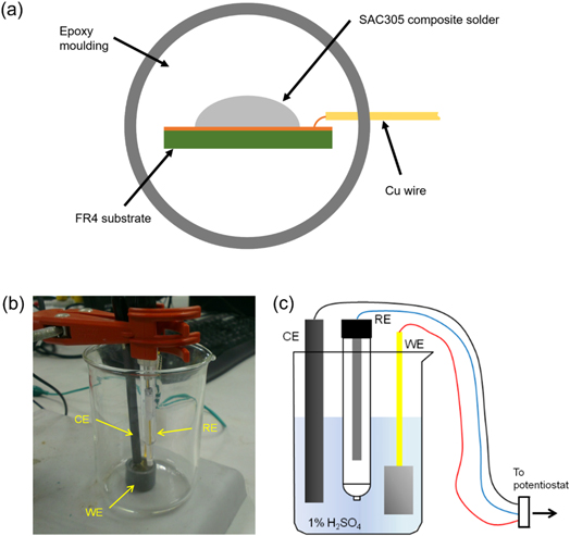
Figure 1. The experimental configuration of the selective electrochemical etching (a) schematic of the working electrode, (b) actual setup and (c) diagram of the setup.
Download figure:
Standard image High-resolution imageA three-electrode setup with 1% H2SO4 electrolyte was used for the initial CV and the electrochemical etching process (figures 1(b)–(c)). The cell consisted of the prepared SAC305/SAC-1.0 T (working electrode), a carbon rod (counter electrode) and a saturated calomel electrode (reference electrode, Koslow). The CV and electrochemical etching process through a CA were conducted by utilizing a potentiostat/galvanostat (Autolab, PGSTAT101). A fixed potential of −350 mV was applied for different etching durations during the etching process (table 1). The CV and CA (at each duration) were repeated for 10 samples in reducing the deviation and ensuring the efficiency of the etching process. The CV and CA curves of the SAC305/SAC-1.0 T were obtained from the potentiostat operating software, NOVA 1.11.
Table 1. Test sample composition and codes.
| Samples | ||
|---|---|---|
| Etching time (s) | SAC305 | SAC-1.0 T |
| 30 | P30 | C30 |
| 60 | P60 | C60 |
| 90 | P90 | C90 |
| 120 | P120 | C120 |
| 150 | P150 | C150 |
The phase and structural analyses were conducted by x-ray diffraction (XRD, Bruker AXS D8 Advance) with monochromatized Cu Kα radiation (λ = 1.5406 Å) in the range of 10° < 2θ < 90°. The morphology of the etched solder was investigated by a Field Emission Scanning Electron Microscope (FESEM, 35VP, Zeiss SupraTM) equipped with energy dispersive x-ray (EDX). Measurement of the IMC thickness were conducted on the obtained images by the ImageJ software. The volume and mass of the removed Sn were determined by first integration of the CA curves through OriginPro software to obtain the charge (Q) values. Faraday's law was then used to calculate the volume and mass.
3. Results and discussion
3.1. Selective electrochemical etching of the SAC305-xTiO2
Electrochemical behavior of both SAC305 and SAC-1.0 T alloys was initially investigated during the selection of the optimum etching potential (figure 2). The CV is essential in allowing the observation on the removal (oxidation) and deposition (reduction) of the phases within the solder alloy with respect to the applied potential. From the CV plots, the solder alloys showed small differences in the electrochemical responses within the evaluated range (−0.74 to 1.86 V). The first and second oxidation peaks are attributed to the co-dissolution of the β-Sn and the IMC phases (Ag3Sn and Cu6Sn5). Reversibly, the reduction peaks correspond well with the co-deposition of these phases. The recorded current for the SAC-1.0 T was found to be slightly higher compared to the SAC305 for both redox reactions. The active dissolution range (highlighted in blue) for the Sn was determined at −0.44 to 0.02 V. The dissolution performance of both SAC305 and SAC-1.0 T alloys was found to be almost identical in this region, as it is visualized from the slope of the curves in the particular region.
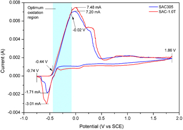
Figure 2. CV curves for the SAC305 and SAC-1.0 T solder alloy.
Download figure:
Standard image High-resolution imageThe absence of electrochemical differences between the solder alloys can be explained by the non-conducting behaviour of the TiO2 nanoparticles. Due to the usage of a non-metal-based electrolyte (H2SO4), no additional reactions were observed apart from the dissolution/deposition of the β-Sn and IMCs, as it is indicated by the two redox peaks. The relatively higher oxidation current (7.48 mA) recorded at the SAC-1.0 T could be attributed to the morphological refinement by the TiO2 nanoparticles. The refinement basically increased the boundary area, which is responsible for better dissolution rate [18]. High dissolution provides a massive supply of Sn in the electrolyte; results in a higher reduction current for the SAC-1.0 T, as it was observed in the CV plot [19].
The highlighted oxidation region (figure 2) indicates the suitable range for determining the etching potential since both SAC305 and SAC-1.0 T alloys exhibited similarities in the electrochemical behaviour. A potential bias of −3.50 mV was found to be optimal considering the relatively low Sn dissolution at this point within the highlighted region. Slow dissolution is important to provide better control of the etching process. It also allows the system to stabilize, thereby provide better consistency during the etching process in comparison to the minimum potential value (−4.40 mV), where the β-Sn dissolution was initiated.
The CA curves obtained at the potential bias of −3.50 mV provided the resultant current, which was comparable to the initial CV analysis for both SAC305 and SAC-1.0 T alloys (figures 3(a)–(b)). The recorded currents have a range from 2.06 to 2.35 mA (SAC305) and 2.25 to 2.36 mA (SAC-1.0 T). The current increases rapidly and then stabilize upon reaching a corresponding value throughout the entire etching process. In average the SAC-1.0 T attained a higher current value (2.30 mA) than the SAC305 (2.19 mA). Neither alloys showed a significant trend for the current with respect to the etching period.

Figure 3. CA curves for the (a) SAC305 and (b) SAC-1.0 T solder alloy obtained at a fixed potential bias of −350 mV.
Download figure:
Standard image High-resolution imageSince current values were comparable with the previous CV (2.18 A) at the etching potential, it indicates that the electrochemical system is consistent. Stability ensures the continuous removal of β-Sn, even in the case of long etching duration, like 150 s. Higher average current at the SAC-1.0 T was expected (similar to the behavior during the CV), due to the more active dissolution of β-Sn, which was caused by the fine grain structure in SAC-1.0 T. The absence of any trend from the CA curve proved that the etching process was not influenced by any other parameters, expect of the addition of the TiO2 nanoparticles and the etching duration.
3.2. Phase and morphology analysis of the etched SAC305-xTiO2
XRD spectra of both SAC305 and SAC-1.0 T solder alloys were normalized after the electrochemical etching prior to the evaluation (figures 4(a)–(b)). The detected phases were β-Sn (ICSD: 98–009–1748), Cu6Sn5 (ICSD: 98–010–0986), Ag3Sn (ICSD: 98–000–1559), SnSO4 (ICSD: 98–009–1957), and TiO2 nanoparticles (ICSD: 98–000–5226). It was found that a prolonged etching duration has two main consequences on the corresponding peaks: reduction of β-Sn and increase of the Cu6Sn5 and Ag3Sn IMC peaks. Another interesting observation was the intensity differences in the different phases. SAC305 presented a relatively high β-Sn count compared to the SAC-1.0 T (and vice versa for the IMC phases).
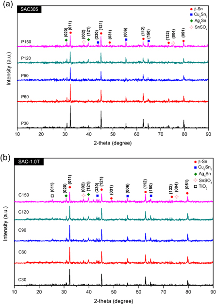
Figure 4. The XRD pattern of the selectively etched (a) SAC305 and (b) SAC-1.0 T solder alloy.
Download figure:
Standard image High-resolution imagePossible formation of new phase was not observed in the case of SAC-1.0 T due to the non-interacting behavior of the TiO2 nanoparticles [20]. The acquisition of the TiO2 peak after 150 s of etching matches to the dominant peak at 2θ = 25.2° [7]. Phase of SnSO4 was found as end by-product of the etching processes. It was caused by the usage of the non-metal-based electrolyte, H2SO4. The gradual reduction in the β-Sn peaks with a longer etching time correlates to the more considerable mass removal of the β-Sn matrix. It matched perfectly with the increases of IMC peaks, which were caused by the further emergence of the IMC phases on the etched surface. The differences in the peak intensities between the SAC305 and SAC-1.0 T reflected the effect of the morphological refinements by the TiO2 nanoparticles [15]. These refinements were also responsible for favoring the removal of the β-Sn matrix.
SEM micrographs of the matrices for both the SAC305 (marked with 'P' in the upcoming micrographs) and SAC-1.0 T (marked with 'C' in the upcoming micrographs) indicated the significant influence of the etching duration on the morphology (figures 5 and 6). Better observation on the shape of rod/thread-like IMC structures (Cu6Sn5 and Ag3Sn) was possible (figures 5(a) and 6(a)) than in the case of the simple chemically-etched samples. After 30 s of etching, the micrographs of P30 (figure 5(b)) and C30 (figure 6(b)) shows small etched regions mainly surrounding the Cu6Sn5 phases. In the case of P60 (figure 5(c)) and C60 (figure 6(c)), larger etched areas were obtained with few remaining β-Sn areas. Etching up to 90 s, (P90 (figure 5(d)) and C90 (figure 6(d)) resulted in a significant amount of β-Sn removal, but the profiles of the edges (mainly the Cu6Sn5) were still rough and uneven. In the case of 30 s and 60 s of etching time, β-Sn matrices were unable to dissolve into the electrolyte. Similarly, the rough edges of the Cu6Sn5 IMC layer were due to the lack of depth between the surface and the background.
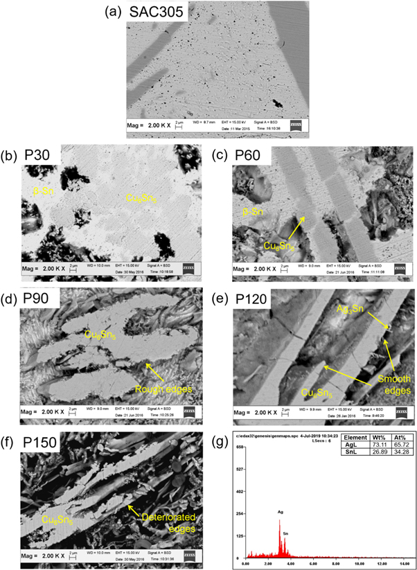
Figure 5. Micrograph of the chemically etched (a) and selectively etched SAC305 (b) P30, (c) P60, (d) P90, (e) P120, (f) P150 with the (g) EDX pattern of the point scan marked in (e).
Download figure:
Standard image High-resolution image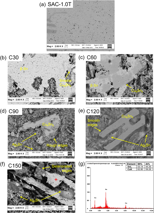
Figure 6. Micrograph of the chemically etched (a) and selectively etched SAC-1.0 T (b) C30, (c) C60, (d) C90, (e) C120, (f) C150 with the (g) EDX pattern of the point scan marked in (f).
Download figure:
Standard image High-resolution imageA smoother profile was obtained in the case of P120 (figure 5(e)) and C120 (figure 6(e)) samples. Improvement was also achieved in the observation of the thread-like Ag3Sn around the Cu6Sn5, as it is shown in both micrographs. A significant difference in depth around the Cu6Sn5 was the key to obtaining an accurate observation of the IMC shapes (as in the P120 and C120 micrographs) [21]. Increasing the etching duration to 150 s caused a significant etching depth increase, as observed in P150 (figure 5(f)) and C150 micrographs (figure 6(f)). However, the prolonged duration also resulted in a deterioration of the Cu6Sn5 IMC phases, since β-Sn initially acted as a supporting structure for the Cu6Sn5 structure. According to the XRD spectra, removal of the β-Sn matrix also helped the detection of the Ag3Sn (figure 5(g)) and Cu6Sn5 IMC phases (figure 6(g)).
According to the calculations, the removed mass and volume of the β-Sn from the SAC-1.0 T was slightly higher compared to the pure SAC305. The most significant differences of the removed mass and volume (5.3% of mas and 5.4% of volume) were observed at the etching duration of 150 s. The more intense removing of β-Sn from the SAC-1.0 T was due to the grain refinement caused by the TiO2 nanoparticles. The grain refinement increases the number of grain boundaries which helps the β-Sn dissolution.
The micrographs at the solder/substrate interfaces clearly show the suppression effect of the TiO2 nanoparticles on the thickness of the Cu6Sn5 IMC layer (figure 7). The IMC thickness in the SAC305 solder joints was between 9.8 to 14.7 μm. In the case of the SAC-1.0 T it was reduced with 50.4% (table 2, figures 7(a) and (b)). It is in relation to the lower diffusion of Cu from the wiring, in the case of composite solders [22]. More intense IMC formation (favored by the TiO2 nanoparticles) adjacent to the diffusion process was generally responsible for reducing the diffusion rate of Cu [23]. The results of the different etching durations were very similar to the results of the Sn matrix etching (figures 5 and 6.). Therefore, we showed only the results of etching duration 90 s and 120 s. Etching duration of 90 s entirely removed the β-Sn regions, as indicated in the images of the P90 and C90 (figures 7(c) and (d)). These provided a better view of the Ag3Sn, but the rough edges of the Cu6Sn5 IMC layer still prevailed. With 120 s of etching time, the elongated P120 (figure 7(e)) and scalloped C120 (figure 7(f)) Cu6Sn5 was easily distinguished and observed. The β-Sn was sufficiently removed, chiefly near the IMC layer, providing smooth edges to the shape of the Cu6Sn5. Besides, the elemental analysis also revealed the trace presence of SnSO4 on the etched surface.
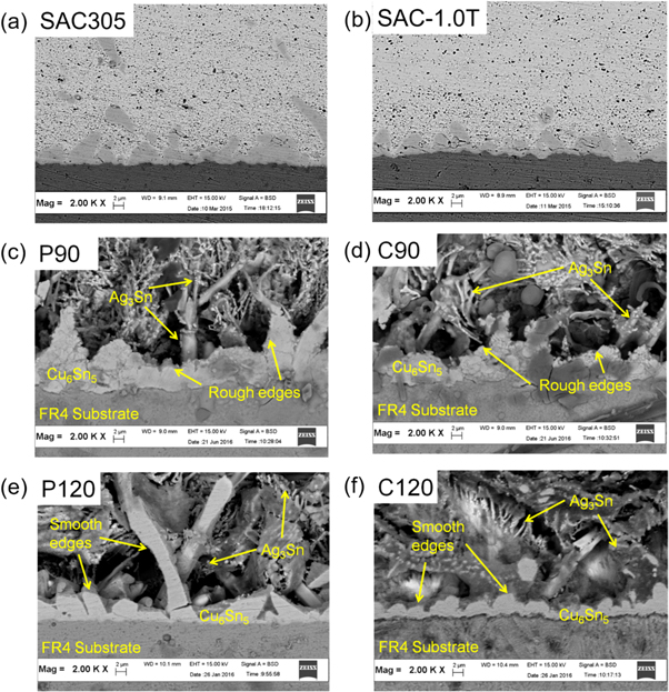
Figure 7. Micrograph of the IMC layer in SAC305 and SAC-1.0 T: chemically etched samples (a) and (b); selectively etched samples (c) and (d) P90, (e) and (f) P120.
Download figure:
Standard image High-resolution imageTable 2. Average thicknesses of the Cu6Sn5 IMC layer in the case of different etching duration.
| Average Cu6Sn5 thickness (μm) | ||
|---|---|---|
| Etching duration (s) | SAC305 | SAC-1.0 T |
| 0 | 11.2 ± 0.567 | 5.7 ± 0.376 |
| 30 | 10.5 ± 0.583 | 7.4 ± 0.337 |
| 60 | 11.0 ± 0.678 | 6.8 ± 0.449 |
| 90 | 12.3 ± 0.377 | 6.3 ± 0.405 |
| 120 | 14.7 ± 0.384 | 3.9 ± 0.287 |
| 150 | 9.8 ± 0.512 | 4.2 ± 0.316 |
The smooth-edged profiles of the selectively-etched C120 significantly enabled good observation of the Cu6Sn5 and Ag3Sn IMC phases (figure 8(a)). This condition was the most suitable for locating and identifying the incorporated TiO2 nanoparticles. The micrographs show most of the TiO2 nanoparticles at the solder/substrate interface. Different cluster sizes of the TiO2 nanoparticles agglomerates (between 116.43 to 334.3 nm in diameter) were observed to be connected to the Cu6Sn5, phases and they were quite distinguishable from the thread-like Ag3Sn (figures 8(b)–(c)). Point EDX scan on the TiO2 cluster indicated the presence of oxygen and titanium (figure 8(d)), while on the smaller cluster the elements that were detected consisted of oxygen, titanium, copper and tin (figure 8(e)). The presence of TiO2 nanoparticles at the solder interface instead of in the Sn matrix can be attributed to the Cu6Sn5 IMC layer [24]. It is most likely that the continuous network of the Cu6Sn5 and the thread-like Ag3Sn acts as an entrapment site for the TiO2 nanoparticles, especially during the flux activation [25]. From the other hand, presence of TiO2 nanoparticles at the solder interface suppresses the growth of the Cu6Sn5 IMC layer (according to the layer thickness decrease), and it is similar to the micrograph obtained in [9, 15]. This behaviour further supports the existence of the TiO2 nanoparticles in this region. Agglomeration during the solid solution condition upon reflow could be attributed to the differences in the sizes of the TiO2 nanoparticle clusters.

Figure 8. Micrographs of the (a) selectively etched C120, (b) magnification images indicated by the red box in (a), (c) magnification images indicated by the yellow box in (a), (d) EDX spectra of the point scan marked in (b) and (e) EDX spectra of the point scan marked in (c).
Download figure:
Standard image High-resolution image3.3. Mechanism of etching in SAC305-xTiO2
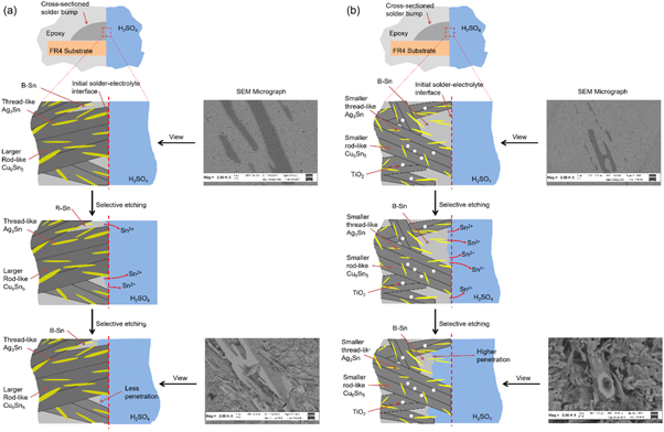
The observed micrographs and the mass/volume calculations indicated the influence of the TiO2 nanoparticles during the selective etching process. The initial condition for both solder alloys is the contact of the polished cross-sectional surface with the H2SO4 electrolyte (figures 9(a)–(b)). The rougher IMCs of Cu6Sn5 and Ag3Sn were mainly exposed at the solder/electrolyte interface prior to the electrochemical etching. Upon the application of the potential bias, selective dissolution of β-Sn into the electrolyte occurred, and produced Sn2+ ions, according to the recorded current of the CA. Since the dissolution of β-Sn from the SAC-1.0 T was more active compared to the SAC305. Subsequently, it resulted in a higher penetration of the electrolyte into the cross-sectioned surface as well (figure 9(b)).
Figure 9. Mechanism of the selective electrochemical etching for the (a) SAC305 and (b) SAC-1.0 T.
Download figure:
Standard image High-resolution image
The etching differences between the solder alloys show the role of the morphology, at the H2SO4 electrolyte interface towards the β-Sn dissolution. The explanation behind the presence of rough or fine IMC phases is related to the density of the grain boundaries. Similar to diffusion (passage of ions), the absence of surrounding atomic bonding at the grain boundaries act as favorable dissolution sites [26]. Unlike continuous bonding inside the β-Sn grains, less energy is required for the β-Sn to leave the system at the weaker points of the matrix (like the defects at the boundaries) [27]. It was confirmed during this study since β-Sn was perfectly removed along the β-Sn and IMC boundaries.
4. Conclusions
Detailed morphologies of the Cu6Sn5 and Ag3Sn were successfully obtained after selective electrochemical etching of SAC305 and SAC-1.0 T solder joints. The non-interacting TiO2 nanoparticles and the use of the non-metal-based H2SO4 electrolyte produced identical phases that were matched by the structural analysis of both the SAC305 and SAC-1.0 T solder alloys. The influence of the etching duration on the morphological analysis was shown by the micrographs, and the most successful observation of the TiO2 near the Cu6Sn5 layer was attained in the case of 120 s etching duration. Applied method has allowed for revealing the clusters of TiO2 nanoparticles entrapped by Cu6Sn5 and thread-like Ag3Sn IMC layer network near the solder/substrate interface. The presence of TiO2 nanoparticles at the solder interface suppresses the growth of the Cu6Sn5 IMC layer. The refined grain morphology of the SAC-1.0 T solder alloy helps the β-Sn dissolution, which results in a higher amount of removed β-Sn. It caused deeper penetration of the etching into the cross-sectioned surface at the SAC-1.0 T than at the SAC305. This effect allows better observation of the IMC phases as well as the TiO2 reinforcement particles in the solder joints.
Acknowledgments
Muhamad Zamri Yahaya and Ahmad Azmin Mohamad appreciate the financial support provided by the FRGS grant 203.PBahan.6071377 (Ref: FRGS/1/2017/TK05/USM/02/2). Balázs Illés appreciates the financial support provided by the National Research, Development, and Innovation Office—NKFIH, FK 127970. Agata Skwarek thanks to the project 006/RID/2018/19 financed in the program 'Regionalna Inicjatywa Doskonałości 2019–2022', Poland.