

Abstract
For the early and easy diagnosis of diseases, we have proposed a silicon photonic biosensor chip with two kinds of MEMS microvalves for a multiple-item detection system. The driving voltage of the vertical type with the circular-plate capacitor structure and that of the lateral type with the comb-shaped electrode are investigated. From mechanical calculations, the driving voltage of the vertical type is estimated to be 30 V and that of the lateral type to be 15 V. The propagation loss at the intersecting waveguides of arrayed ring-resonator biosensors is also estimated. In the case of optimized intersecting waveguides, more than 67% transmittance of TE-mode light is simulated for the series connection of 20 intersecting waveguides. It is confirmed that it is possible to fabricate an 8 × 12 arrayed biosensor chip in an area of 1 × 1.5 mm2 taking the device size of the microvalves into consideration. We have, for the first time, designed a whole system, including sensors and a fluid channel with MEMS microvalves.
Export citation and abstract BibTeX RIS
1. Introduction
Biosensor chips for the diagnosis of diseases are desired especially for the aging society to realize simple and easy detection systems. Enzyme-linked immunosorbent assay (ELISA)1–4) is a well-known detection method for the diagnosis of diseases, where an antigen or an antibody is labeled with an enzyme or a fluorescent material. In other optical biosensors,5) although surface-plasmon resonators (SPRs),6–8) optical fibers,9–11) and anomalous reflections of gold12) have been studied, they generally require a large external optical system. For early and easy diagnosis, silicon photonic devices fabricated using Si technologies have been used as immunoassay biosensors owing to their advantages of low cost and small size, and single-item detection has been successfully demonstarated.13–21) Moreover, these advantages enable the easy integration of photonic devices, and multiple-item detection is expected. Figure 1 shows the basic concept of a multiple-item detection system consisting of an array of ring-resonator biosensors. Different biomaterials are set on each biosensor by solution flow control using micro-electro-mechanical system (MEMS) microvalves in a fluid channel. The specified optical signal from a biosensor with the target biomaterial is selected using ring-resonator wavelength selection filters.
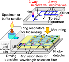
Fig. 1. Basic concept of multiple-item detection biosensing system.
Download figure:
Standard image High-resolution imageTo realize this chip, fabrication technologies for arrayed ring-resonator biosensors, fluid channels with MEMS microvalves, and photodiodes, and further progress in the bonding technology for laser diodes are necessary. In this paper, we especially focus on MEMS microvalves and investigate the design of an arrayed biosensor chip with a fluid channel. The further detailed and exact discussion is an expansion of our previous report.22) Moreover, the propagation loss at the intersecting waveguide is discussed. Two kinds of microvalves, the vertical and lateral types, are considered as shown in Figs. 2 and 3. For low-voltage operation, the valves consist of a photoresist (SU-8). Al electrodes in the fluid channel are covered by the SU-8 photoresist because solutions for biosensing are generally electrically conductive. In Fig. 2, a solution is input from the inlet and passes vertically through the valve area and out through the outlet. During voltage application, electrostatic force is induced in SU-8 photoresist layers between the electrodes of a parallel circular plate. The force is attractive and the valve moves vertically until the valve touches the bottom SU-8 layer. Then, the solution flow is stopped. The electrostatic force is designed to be larger than the force generated by the deformation of the valve. In Fig. 3, the solution is also input from the inlet and passes laterally through the valve area and out through the outlet. During voltage application, the electrostatic force between comb-shaped electrodes is attractive and the valve moves laterally. The solution flow can be stopped by the valve. Low-voltage valve operation is expected, because Young's modulus of a photoresist is generally smaller than that of a nonorganic material such as silicon and the valve area can be deformed at a low voltage.
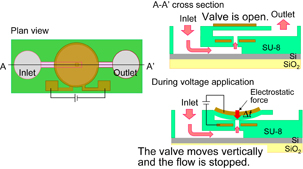
Fig. 2. Schematic image of vertical-type valve and driving mechanism of valve part.
Download figure:
Standard image High-resolution image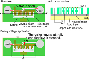
Fig. 3. Schematic image of lateral-type valve and driving mechanism of valve part.
Download figure:
Standard image High-resolution imageThe fabrication of arrayed ring resonators is possible using the same fabrication process for a single ring resonator. The noted difference is the existence of intersecting waveguides. The propagation loss increases when the numbers of arrayed ring resonators and intersecting waveguides increase. We also discuss the propagation loss at the intersecting waveguide in Sect. 3.2.
2. Design parameter for calculation and simulation method
To evaluate the proposed microvalves, the voltage dependences of the maximum displacement of movable parts are calculated. The detailed design parameters are shown in Fig. 4. The movable part of the vertical-type microvalve is the upper circular plate and that of the lateral-type microvalve is the movable finger of the comb-shaped electrode. In the lateral type, to reduce the operation voltage, the fixed fingers are arranged in not only the lateral direction but also the vertical direction. For the mechanical calculation, the physical constants of the SU-8 photoresist and Al are assumed as follows: relative permittivity of SU-8, ∼3;23,24) Young's modulus of SU-8, ∼4.4 GPa;25,26) Poisson's ratio of SU-8, ∼0.26;27) Young's modulus of Al, ∼70.3 GPa; Poisson's ratio of Al, ∼0.345.
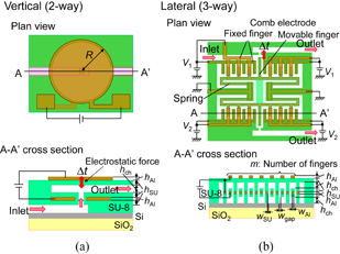
Fig. 4. Detailed structures of (a) vertical-type and (b) lateral-type valves.
Download figure:
Standard image High-resolution imageFor a low propagation loss, we consider the well-known shape of the intersecting waveguides shown in Fig. 5. The thickness of the top silicon layer of a silicon-on-insulator (SOI) wafer (300 nm) is different from that used by another research group (220 nm).28) Biomaterials can be adsorbed at the waveguide surface except at the lower cladding side. A portrait shape has a larger surface area where biomaterials can be adsorbed than a landscape shape. This indicates that the waveguide of 300 nm thickness can adsorb larger amounts of biomaterials than that of 220 nm thickness. The sensitivity of biosensors is also expected to be higher. Using the design parameters shown in Fig. 5, the propagation loss is simulated using the finite-difference time-domain method (RSoft Design Group FullWave).
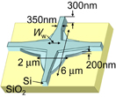
Fig. 5. Schematic image of intersecting waveguide.
Download figure:
Standard image High-resolution image3. Results and discussion
3.1. Driving voltage of microvalve
To estimate the driving voltage necessary to close the valve, the voltage dependence of the displacement of a valve part is calculated.
3.1.1. Vertical-type microvalve.
The voltage dependence of the maximum displacement of the vertical-type valve is shown in Fig. 6 as a parameter of the height of SU-8, hSU. A clamped circular plate is used and the maximum displacement Δt is calculated from the electrostatic force per unit area, p, and flexural rigidity, D. It is given by


where R, Ec, hc, and νc are the radius of the circular plate, Young's modulus, thickness, and Poisson's ratio of a composite membrane, respectively. The composite membrane forms the movable valve part, which consists of SU-8 and Al. The Young's modulus and Poisson's ratio of the composite membrane are assumed to be weighted averages.29) It is given by


where E, h, and ν are Young's modulus, thickness, and Poisson's ratio, respectively. The subscripts SU and Al denote the SU-8 and Al layers, respectively. The electrostatic force is given by the movable direction differential of capacitive energy. The movable direction is vertical and the equation is given by

where S, W, d, ε, and V are the circular-plate area, the capacitive energy, the distance in electric field generated by the electrodes of the circular plate, the permittivity, and the driving voltage, respectively. In the vertical type, ε is the permittivity of SU-8 and d is two times hSU because the fluid channel is filled with a solution that is generally conductive. In Fig. 6, the radius of the circular plate (R) and the height of the Al layer (hAl) are fixed at 50 and 0.1 µm, respectively. The considered distance between the electrodes of the circular-plate capacitor is <2 µm, which is the same as the height of the fluid channel. A displacement of 3 µm is sufficient to close the valve. When hSU is 0.5 µm, more than 3 µm is obtained at a driving voltage of 30 V. In general, operation voltage of MEMS devices tends to be large (∼100 V).30,31) In contrast, when the device size is large, the operation voltage is low. The operation voltage and size of the proposed device are suppressed to be 30 V and 50 µm in radius, respectively.
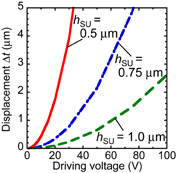
Fig. 6. Calculated voltage dependence of displacement for vertical-type valve.
Download figure:
Standard image High-resolution image3.1.2. Lateral-type microvalve.
The voltage dependence of displacement of the lateral-type valve is shown in Fig. 7 as a parameter of the number of fingers, m. The shape between the movable fingers and the anchor part is similar to a folded beam and a spring structure is formed. The displacement Δt is calculated from the spring constant k, which is given by


where F, W, C, and t are the electrostatic force, capacitive energy, capacitance, and position coordinate of movable direction, respectively.32,33) The spring constant is given by

where τb, wb, and lb are the thickness, width, and length of the beam forming the spring structure, respectively.34) In Fig. 7, the width of the Al layer (wAl), the height of the Al layer (hAl), the width of SU-8 (wSU), the height of SU-8 (hSU), and the gap between fingers (wgap) are 2.0, 0.1, 0.5, 0.5, and 1.0 µm, respectively. In the lateral type, the differential of capacitance is given by

where the term wAl/2hSU denotes the capacitance between the upper electrodes and the movable fingers, and the term hAl/wSU denotes the capacitance between the fixed fingers and the movable fingers. Other values are given by


When m is 75, which implies a large device length of 2lb ∼ 600 µm, more than 3 µm is obtained at a driving voltage of 15 V. The length in the other direction can be fixed and the whole lateral-type microvalve is rectangular, while the required area for the single-ring resonator is similar to a square, which is ∼30 × 30 µm2. Valves of the vertical and lateral types are used for different purposes. Vertical-type valves (100 × 100 µm2) are used for the solution flow control of each biosensor, and the lateral-type valves are used for branches at the upper stream, as shown in Fig. 1, where the remaining region exists. Whereas the vertical type is a two-way valve, the lateral type can be a three-way valve because one more pattern can be arranged symmetrically on the lower side as shown in Fig. 3. Solution flow can be controlled by the voltages V1 and V2 in Fig. 4.
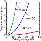
Fig. 7. Calculated voltage dependence of displacement for lateral-type valve.
Download figure:
Standard image High-resolution imageAn 8 × 12 array is often used for arrayed biosensors, for example, the 96-well plates used in ELISA. We also consider 8 × 12 arrayed ring-resonator biosensors. The vertical-type microvalves are arranged at each ring-resonator biosensor, then the smallest chip size is 0.8 × 1.2 mm2 because the size of one vertical valve is 0.1 × 0.1 mm2. The realistic size including the remaining area is ∼1 × 1.5 mm2. Although the device size is small and the operation voltage is low, the actual fabrication process becomes complex. We have fabricated the desired structure by forming multilayers of SU-8 and spin-on-glass (SOG). After the selective HF etching of the SOG layer, a fluid channel with the valve structure is fabricated. At present, the fabrication of the desired structure has almost been achieved. The fabrication and operation will be reported elsewhere.
3.2. Propagation loss caused by intersecting waveguides
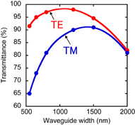
Optical signal intensity from a specific ring-resonator biosensor decreases after propagating in many intersecting waveguides. Figure 8 shows the transmittance of a single intersection of waveguides. The simulation of transmittance is carried out using the design parameters shown in Fig. 5. The intersection part of the waveguide consists of a waveguide of 200 nm thickness and another of 300 nm thickness. The waveguide of 200 nm thickness has two arcs with a radius 5 µm, and the vertical and horizontal sizes are 6 and 2 µm, respectively. The width of the waveguide of 300 nm thickness becomes Ww linearly from 350 nm. A light is input from one side of the intersecting waveguide and light propagation is monitored by finite-difference time-domain simulation. The light propagation modes of near-field and optical intensities are monitored at several points. By monitoring on the opposite side, the propagation mode and transmittance are estimated. In the TE mode, 98% of an optical signal is transmitted after propagating in a single intersection of waveguides when the width Ww is ∼1100 nm. For the 8 × 12 arrayed ring-resonator biosensors, the lowest transmittance after propagating in the biosensor chip is 67%, which is given by (0.98)20 ∼ 0.67 because the largest number of intersecting waveguides is 20. This value seems sufficient for biosensing. In the TM mode, the highest transmittance of a single intersection of waveguides is 92%. Then, the lowest transmittance after propagating in the biosensor chip is 19%, which is given by (0.92)20 ∼ 0.19. From these results, the TE mode is superior to the optical mode in the arrayed biosensor chips.
Fig. 8. Simulated transmittance of a single intersection of waveguides.
Download figure:
Standard image High-resolution image
4. Conclusions
We have investigated MEMS microvalves for solution flow control in multiple-item detection biosensor chips. The driving voltage of the vertical-type valve is estimated to be 30 V and that of the lateral-type valve is 15 V. After considering the device size, it is possible to fabricate an 8 × 12 arrayed biosensor chip in an area of 1 × 1.5 mm2. In the case of optimized intersecting waveguides, more than 67% of optical signal transmittance is simulated in the TE mode for an 8 × 12 arrayed biosensor chip. For the practical use of multiple-item silicon photonic biosensor chips, both the sensors and a flow control system are necessary to be integrated on a chip. In this paper, we have, for the first time, designed a whole system including sensors and a fluid channel with MEMS microvalves.
Acknowledgment
This work was supported in part by a Grant-in-Aid for Young Scientists (B) (No. 16K21191) from the Japan Society for the Promotion of Science.