

Abstract
The transport properties of the percolation channels of memristive structures based on YBa2Cu3O7−δ epitaxial films were studied. Molecular electronics and Andreev reflection spectroscopy were utilised, and the influence of the superconductive transition of electrodes on resistive switching effects in these structures was examined. Based on the analysis of the conductivity mechanisms in the obtained heterostructures, it is assumed that percolation channels form through a chain of domains disordered by oxygen about 10 nm in diameter, with a maximum Tc of 60 K. Zero-bias anomalies of the dynamic resistance of the studied structures display temperature dependence of the critical current of typical superconductor—normal—superconductor weak links within the framework of Kulik–Omel'yanchuk theory in the dirty limit. A simulation was used to determine the physical parameters of the studied heterostructures.
Export citation and abstract BibTeX RIS
1. Introduction
One of the tasks of modern physics is concerned with the search for new physical phenomena and the possibility of realizing them in various applications. In this regard, the bipolar effects of resistive switching (BERS) in heterogenous structures of different compounds are considered and even used practically as new generation memory elements (memristors) [1–8].
The current state of the matter is focused on searching for different heterostructures with the above-mentioned property. Almost all materials with a strongly correlated electronic system display the switching effect to some extent in the presence of the asymmetry of the electric contacts. Presently, there is no absolutely clear idea regarding the origin of the switching. It seems important to distinguish the physical character of resistive switching in structures containing strongly correlated electronic systems, which would support finding optimal heterostructures, and, moreover, this will assist in leading to an understanding of the character of the formation of the functional properties of these materials. A memristor can be defined as a passive element of an electric circuit, whose resistance depends on a charge passed through it. After the voltage in the circuit is switched off, a memristor does not change its state, i.e. it 'remembers' the last value of resistance ('ON' or 'OFF' state). Further studies have shown that properties of the memristor allow its application as a switch, being a ReRAM element. Up until now, none of the theoretical models can explain the switching phenomenon entirely because of a lack of a fundamental understanding of the resistive switching process. In order to precisely explain the acting principles, it is necessary to consider, comprehensively, the switching mechanism of the resistance at the atomic level, i.e. how conductive pathways form and decompose.
The effect of resistive switching is observed in a wide range of structures with an insulator layer consisting of simple oxides or of complex compounds. In previous works [9, 10], while studying BERS in the structures based on high temperature superconductive films, it was shown how memristor structures can be formed using the functional properties of high temperature superconductors (HTSC). Two important factors should be highlighted. First, paternal HTSC compounds are antiferromagnetic Mott isolators, and the metal–insulator transition is realized upon doping them with oxygen [11]. This circumstance is a key functional property of HTSC used for making heterostructures with BERS. As follows from the YBa2Cu3O7−δ (YBCO) phase diagram [11], YBCO containing 0–6.5 oxygen is an insulator—namely, the YBCO6 phase—while if oxygen content is from 6.56–7, YBCO is a superconductor—namely the YBCO7 phase. Secondly, all studied heterostructures can be selected as structures with vertical or planar geometry. The first type includes symmetric metal–insulator–metal (MIM) junctions having micro and nanometer sizes. Planar structures also demonstrate MIM transitions, but only with micro size forms by a point-like top electrode. In [9], it was shown that in such planar structures, resistive switching was substantially affected by the topology of the electric field distribution. It was also shown that an important condition for the effect to be detected was the existence of a surface layer deficient by carriers over about the 10 nm region with the resistance different from the bulk. The bipolar effect of the resistive switching manifests itself in a change of HTSC-normal metal heterojunctions (HJs). At a certain polarity of the electric field, there is a change in the phase composition of the HTSC surface layer at the nanometer scale. As a result, metastable high-resistive (OFF) and low-resistive (ON) states of a heterojunction are realized, and a colossal electrical resistance (CER) arises [3]. CER is the ratio between resistivities in the OFF and ON states, and it characterizes the form memory effect. The switching effect of the resistive properties of HJs under action of an electric field, which is considered in the discussed works, provides evidence in favor of the so called filamentary model with electroforming. The most popular approaches to understanding the resistance switching mechanisms are models based on the formation and breakage of conductive filaments upon the change in the concentration of oxygen vacancies in the 'conductivity channels'. Lately, a few studies have appeared concerning technologies of non-filamentary energy-independent memory production based on the metal–insulator Mott transition in nickel oxide and other junctions in metal compounds [12, 13].
The YBCO system was also actively studied as a memristor option, first in microcontacts and then in film heterostuctures produced by a modern lithography technique [14–20]. It is reported in [17] on BERS observed in YBa2Cu3O6+δ/Nb-doped SrTiO3 heterojunctions. The current–voltage characteristics (CVCs) of these heterojunctions show hysteresis which increases, while the temperature and the oxygen content decreases. In [18], dynamical behavior of the resistive switching in ceramic YBCO/metal interfaces was involved and a circuit model with two parallel diodes and resistances was developed, which represented very well the non-linear current dependence of the differential resistance. A similar model of two diodes switched towards each other was applied to approximate the current transfer of the metastable high resistive states in heterojunctions incidental to the HTSC epitaxial films in our previous work [9]. It has been shown that CVCs of the structures point to the presence of the sequential resistance, Rs, which is the spread resistance, and parallel short-circuits, Ri, which should be taken into account, while modelling the transport properties of the studied structures using the relation:
where I0 = A * T2 * S * exp (−(e фв/kT)), A is the Richardson constant, S is the area of the contact, фв is the barrier height.
CVCs and the temperature dependence of the resistance, R(T), of Au/YBa2Cu3O7−δ interfaces were studied in different resistive states in [20]. These states were obtained through resistive switching after N cyclic electric pulses with different voltage amplitudes. The CVC and the R(T) dependencies of different states are described within frameworks of the Poole–Frenkel (P–F) mechanism with the capturing energy of the levels Et in the range of 0.06–0.11 eV. The presence of the P–F mechanism proves the existence of an oxygen-deficient YBCO layer close to the interface. As a result, the electric transfer of these structures was determined by a degree of disorder and by the energy level of the traps. In different temperature ranges, non-linear effects in the electric conductivity are related either to the P–F emission or to the hopping mechanism of electronic transport. The contemporary studies of a memristive structure have no data on the real distribution of the electric field in the structures, which contain various kinds of defects or several interfaces. Specifically, the electric field distribution, which depends on the resistive properties of the different transition areas, and, in turn, changes in these resistive properties during switching, determine the dynamic of resistive switching. It should be noted that, throughout, the current field is implied as E(x, y, z): J = σ * E, which cannot always be determined, and is taken commonly as E = V * e/d, where V is the applied voltage to a structure at step d. The importance of this circumstance should be highlighted. In most works, the distribution of the electric field in a structure is not analyzed, and this distribution changes during switching. In our work [9], it was shown, using computation, that in planar structures, the resistive switching is substantially influenced by the topology of the electric field distribution. An essential condition for the detection of the effect is the presence of a surface layer (deficient by carriers) of dimensions of about 10 nm with the conductivity differing from the bulk value. In this case, the heterogeneous electric field distribution creates areas with higher electric field intensity (critical areas), and a ring-shaped percolation path forms at the edge of the top contact [9].
The present work aims at studying the transport properties of the percolation channels of the memristive structures based on YBCO epitaxial films in order to find the mechanism of the formation of such channels. The molecular electronic tools, Andreev reflection spectroscopy, and the effect of the superconductive state of electrodes on resistive switching effects in these structures, were applied to use the metastable ON state in a heterostructure as a weak link between the HTSC film and the metallic electrode to detect the Andreev reflection and the weak link effects.
In this work, the heterostructures in a planar geometry were used. Simulation methods were used to describe the studied effect. Computer modeling can substantially accelerate the choice of the physical models, adequately describing the bipolar resistive switching in the heterostructures based on the oxide compounds. Thus, in previous works, we have accounted for the influence of the heterogeneous distribution of the electric field in the metal–oxide–metal heterostructure. In particular, the electric field distribution forms and, to a large extent, predetermines the switching process as the voltage is sweeping in a heterostructure. It has been shown that in structures with a point-like electrode, a conducting channel forms and breaks at the edge of the metallic electrode. Following these considerations, the studied structures obtained in such a planar geometry are sensitive to changes in the resistive properties of different areas of a structure which change under the action of the electric field, the temperature, and consequently, the potential distribution of the electric field and the conductive routes change. Therefore, it is important to control these changes, and to do so, the simulation methods were developed for the numerical calculation of the given heterostructures.
2. Experimental
Epitaxial films YB2C3O7−δ(YBCO) with a maximal critical temperature of superconductive transition (Tc) were obtained by a pulse laser deposition technique. The substrates were SrTiO3 (100) single crystals 5 × 10 mm2 in size. The quality of the films was examined by x-ray photoelectron spectroscopy. Details of the films' production and the formation of the heterostructures are described in [10]. The x-ray analysis detected the presence of a dielectric phase on the surface of the obtained YBCO films, in which (according to [21]), a correlation was found between the unit cell parameter c and the oxygen content in YBa2Cu3O7−δ.
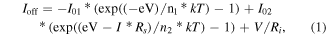
The mesoscopic heterostructures were of two types: the first were of a microcontact type, and the second were produced by photolithography. Microcontacts were obtained by driving a metal needle into a micro-handler onto the surface of an as-grown film, or, otherwise, silver was sputtered over a mask. Figures 1(a)–(c) show the schemes of the cross sections of the initial films, the microcontacts, and of the heterostructure obtained using photolithography. It should be noted that a method important for these studies was used where the silver electrodes were 'burned' into the YBCO film by pulsed laser deposition in order to avoid undesirable contact resistance and to realize a planar geometry of the current spread. The lithography formed a Ag/YBCO6 /YBCO7 structure which had a contact window of 100 × 100 μm2 or 50 × 50 μm2. The obtained heterojunctions were studied to find the existence of resistive switching, CVCs, and the temperature dependence of the resistance of the structures. By changing the external parameters—the frequency and amplitude of the electric voltage applied to a heterojunction—new metastable states were realized.
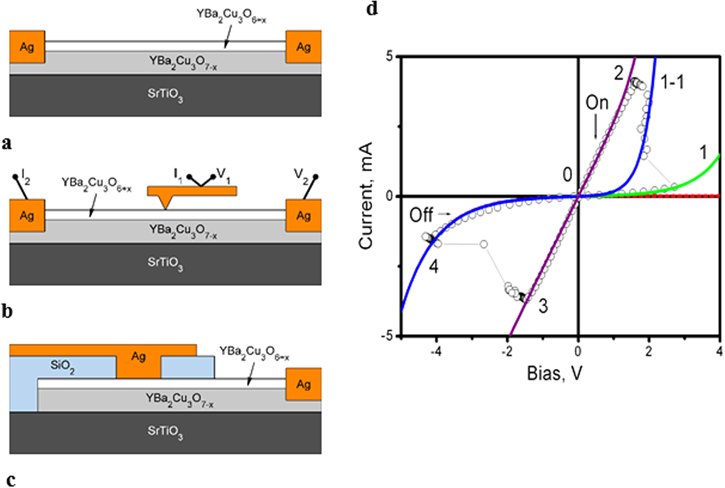
Figure 1. (a) The scheme of the initial film. Its size is 1.0 × 0.5 cm2, the thickness of the YBCO7 superconductive film is about 200 nm, the thickness of the dielectric part of the film is about 30 nm (according to estimations made in [10]). (b) The microcontact structure. (c) A scheme of a lithographic planar-type structure with a Ag film electrode. (d) Example of CVC heterostructures of planar type, such as Ag/YBCO6/YBCO7 (T = 300 K).
Download figure:
Standard image High-resolution imageFigure 1(d) shows an example of CVCs with switching in Ag/YBCO6/YBCO7 heterostructures obtained using photolithography. The obtained heterostructures stably display the effect of resistive switching for more than 100 cycles with the ratio of resistances ROFF/RON ∼ 10–100 provided that the current is limited up to 10 mA. As the current increases further, the structures can degrade.
Figure 2(a) shows the temperature dependence of the resistance of the initial film in the [110] direction and the metastable states of the mesoscopic structure are realized in this work. Each metastable state was obtained within the limited current mode. Curve 1 was measured using a four-point technique along the film area; the measuring scheme is shown in figure 2(b). The measuring scheme of the metastable states is shown in figure 2(c).
Figure 2. (a) Temperature dependencies of resistances: (1) initial YBCO film of the [110] direction; (2, 3, 4, 5, 6) are metastable ON states; (7) is the metastable OFF state in the [001] direction. (b) The measuring scheme; curve 1 was measured using a four-point method along the film plane. (c) The measuring scheme of metastable states 2, 3, 4, 5, 6, 7.
Download figure:
Standard image High-resolution imageAs is shown in figure 2, several metastable ON states which display the superconductive transition are observed. It is also important that a superconductive transition shows the two-phase character of superconductivity in a channel. It means that there are areas in a percolation channel containing different amounts of oxygen.
Each metastable state was swept by the voltage simultaneously with temperature to detect the dynamic resistance. Studies of the dynamic resistance Rd = dV/dI(V, T) of the structures; the normal metal-superconductor is an efficient tool for tracking the order parameter (superconductive energy gap) in the Andreev reflection effect [22]. Many attempts were made in previous work to find the order parameter in the HTSC–normal metal structures using a microcontact and tunneling spectroscopy [23]. Figures 3, 4 show examples of the dynamic resistance of the metastable states of the structure, Rd = (dV/dI(V)), on the temperature with zero anomalies of the Andreev reflection type.
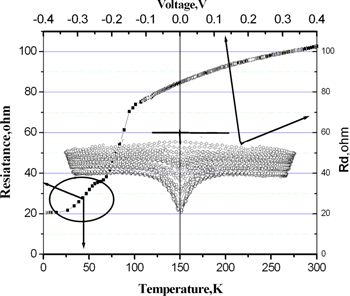
Figure 3. An example of the temperature dependence of the resistance of a metastable ON state and zero anomalies in dynamic resistance Rd associated with the breakage of weak links in the superconductive channel.
Download figure:
Standard image High-resolution image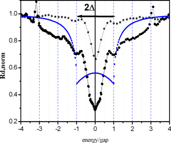
Figure 4. Dependence of the dynamic resistance of YBCO on energy (normalized by gap Δ = 19 meV [22]) for the metastable states with the residual resistance R1 = 1 Ohm (filled circles) and 3.5 Ohm, (filled asterisks) T = 4.2 K. The dashed line shows the theoretical dependence in the Blonder–Tinkham–Klapwijk model (BTK). The BTK parameter is Z = 0.4.
Download figure:
Standard image High-resolution image3. Calculation and discussion
The experimental results indicated that the reproducible BERS were detected on Ag/YBCO film heterojuctions of planar type and were stable. A CVC with BERS demonstrated a diode behaviour. The current flow in the metastable high-resistive states of the studied HJ was approximated by the behavior of two oppositely connected parallel diodes described by equation (1) (figure 1). Furthermore, the low temperature, 60 K YBCO phase contributed to the resistance of the channel in the metastable ON states. The CVC approximation following equation (1) is shown in figure 1.
In order to explain the switching mechanism, we shall consider components which comprise the resistance of the transition, and the characteristic of the electric field influence on them.
The temperature dependence of the resistance of the metastable states Roni provided the possibility of disclosing contributions from the components of a structure to resistance. Referring to figure 2, one can see that the temperature dependence of the resistance correlates with the behavior of the YBCO thin films and has three specific components: R1 is the residual resistance of a percolation channel, R2 is actually the resistance of the percolation channel, R3 is the resistance resulting from the transition of a YBCO basic film into the superconductive state.
Based on the model of the critical electric field [9], the numerical simulation was used to determine the parameters of the studied contacts (figure 5, table 1). The mathematical model is based on Poisson's equation:

that enables the determination of the potential distribution ϕ(r, z) and then the field distribution, E (strength), by the distribution of specific conductivity σ(r, z) in the heterostructure. The shape of the conductive channels was found by the following algorithm: (1) The distribution of the electric potential ϕ (r, z) is calculated from the actual distribution of the specific conductivity σ in the structure; (2) the distribution of the electric field intensity E(r, z) is determined; (3) if there are areas in the defective layer in which ∣E (r, z)∣ ≥ Ecritical, σin is replaced by σout (σin and σout take the values σon or σoff depending on the bias polarities) and the procedure returns to step (1).
Table 1. The calculated and experimental data (T = 300 K).
| R1 (Оhm) | Roff (Оhm) | Ron (Оhm) | CER | ro (cm) | Δr (nm) | R2 (Оhm) | R3 (Оhm) | Ron (cal) |
|---|---|---|---|---|---|---|---|---|
| 1 | 500 | 24 | 20 | 10−3 | 40 | 2 | 20 | 24 |
| 9.4 | 600 | 68 | 9 | 10−3 | 30 | 4 | 55 | 68 |
| 20 | 1000 | 107 | 10 | 10−3 | 36 | 16 | 71 | 107 |
| 135 | 18 000 | 290 | 62 | 10−3 | 46 | 94 | 61 | 380 |
| 430 | 30 000 | 719 | 42 | 10−3 | 45 | 135 | 144 | 716 |
Roff, Ron—the resistances of the heterostructure metastable states. r0—the radius of the top Ag electrode. Δr—the thickness of the conductive channel. R1—the residual resistance of the conductive channel. R2—the resistance of the conductive channel. R3—the resistance of the YBCO film. Ron(cal) = R1 + R2 + R3.
In figure 5, the main branches of the CVC of the heterojunctions with switching are displayed (the arrows show the sweep directions). The high-resistive state was determined by the barrier properties of the structure—branch 4–0–1 on the CVC (figure 1). In point 1, the tunneling of the carriers begins, and the properties of the heterostructure change. The resistance decreases (branch 1–2), in this case by an order of magnitude. Then the low-resistive state occurs (branch 2–3), and then the transition in the high-resistive state takes place on branch 3–4. Branches 4–1 and 2–3 are reversible; switchings exist on branches 1–2 and 3–4. At that, it is absolutely clear that without involving electrodiffusion, which changes a charge state in the active region of the transition, it is impossible to explain the polarity and reversibility of the switchings. To make a switching reversible, a structure should meet some topological demand, i.e. the electric field distribution should be such as to reach the electric field intensity in the voltage sweeping key points, high enough for oxygen electrodiffusion.
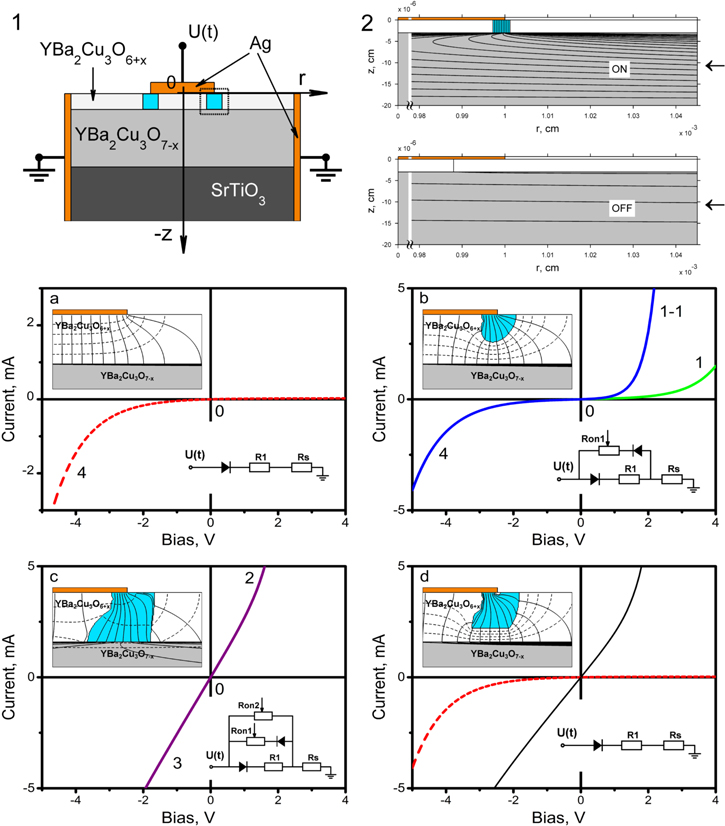
Figure 5. (1) The scheme of the structure. The area highlighted by the dashed rectangle is the active part of the structure—the region presented in (a)–(d). (2) An example of the calculation of the distribution of the current and the potential lines during the formation of metastable ON and OFF states. The arrows show the areas of the spread current in the ON and OFF states. These areas contribute to the total resistance of the ON state via R3 (a)–(d) diagrams and the equivalent schemes of the main branches of the CVC (figure 1) of the heterojunction with resistive switchings. The upper insets present different stages of the formation/decay of a conducting channel in the area highlighted by the dashed rectangle in (1). The critical area model [9] is used for simulation. Dashed lines in the insets are equipotential lines, solid lines are lines of current flow. (a) CVC branch '0–1' and equivalent scheme; (b) CVC branch '1–2–3' and equivalent scheme, formation of Ron1—fast process, formation of Ron2—slow process; (c) CVC branch '3–4' and equivalent scheme; (d) CVC branch '4–0' and equivalent scheme.
Download figure:
Standard image High-resolution imageThe calculated and experimental data (T = 300 K) are listed in table 1.
Therefore, as the surface layer is in a low-resistive state, a conducting channel forms, shaped as a ring with cross-section sizes of about r = 10 μm, Δr ∼ 50 nm, L ∼ 30 nm. The temperature dependence of the resistance of the metastable states Ron provides the possibility of disclosing contributions from components of a structure to resistance.
According to the numerical calculations, the major contribution to the resistance makes the spread resistance in the basic film, R3. This is very interesting and is as a result of a special character in the spreading in the planar geometry; the current inflows in the basic film through a contact of the ring-shaped percolation channel (with superconductive critical temperature Tc ∼ 90 K (inset 2 in figure 5)). Thus, Ron is predetermined by the resistance of the percolation channel R2 (with Tc ∼ 60 K) and by the current spread resistance R3 (with Тс ∼ 90 K).
As can be seen from the temperature dependence of the percolation channel resistance, the low-critical temperature 60 K YBCO phase contributes to the resistance of the channel. This circumstance is very important. From these structural studies of the effect of non-stoichiometry by oxygen on the critical temperature of the superconductivity transition (Tc), the correlation between Tc and δ parameter becomes known [21]. The structural properties of the oxygen deficient YBa2Cu307−δ compounds were found using neutron powder diffraction for 0.07 < δ < 0.91 compositions, and they explain certain behavior of the plateau in the dependence of Tc on δ.
As is known from [21, 24, 25], the phase with Tc = 60 K is the disordered phase consisting of domains with different oxygen stoichiometry. It is assumed that the interior and the exterior areas of the domains are different depending on the oxygen content, and the observed 60 K plateau could be associated with the existence of small (<100 Å) domains in the phase-decomposed medium. This confirms our model of the critical electric field region for percolation channel formation.
Figure 3 shows that in the dependence of the dynamic resistance of the metastable states on the temperature, there is a zero anomaly, which extinguishes with temperature. These anomalies are usually interpreted as the Andreev reflection (figure 4). It is seen that special features in the dynamic resistance are in the range of gap energies, but the experimental data differ from the theoretical. Provided that a disordered phase forms in the percolation channel, we shall assume that zero anomaly is a result of the breakage of the weak links between superconductive domains, and we shall estimate the critical current of the process.
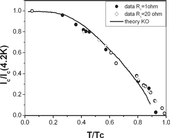
Figure 6 shows the dependence of the normalized critical current of the metastable ON states on the temperature and the theoretical dependence of the critical current of weak links in the Josephson superconductor–normal metal–superconductor (SNS) in Kulik–Omel'yanchuk theory (KO) [26, 27]. The KO theory is correct for the short links approach, i.e. L/ξ < 0, (L is the length of a link, ξ is the coherence length). It would be difficult to estimate this ratio in our case. Despite the KO model describing our data quite comprehensively, there are many open questions remaining: which part of the channel contains a weak link, which are L and ξ parameters, what Josephson properties has the percolation channel, etc. Therefore, the presented results do not provide us with an ultimate conclusion regarding the Josephson character of weak links in the percolation channel, and hence additional studies are necessary.
Figure 6. The symbols represent the normalized critical current depending on the temperature of the heterostructure in the metastable ON states. The solid line is the temperature dependence of the critical current predicted by Kulik and Omelýanchuk for weak links SNS in the dirty limit [26].
Download figure:
Standard image High-resolution image
4. Conclusions
Thus, the high-resistive OFF state in memristive YBCO heterostructures is determined by the barrier properties of a structure. The heterogeneous distribution of the electric field near the electrodes creates areas with higher electric field intensity, characterized by the motion and the redistribution of oxygen defects in the surface layer of the film and a change in the resistive properties of all the structures. The percolation channel is formed by a chain of oxygen-disordered domains under the action of several processes: the formation of tunnel channels on electrodes of the structure and oxygen electrodiffusion to oxygen vacancies. The critical temperature of the superconductive transition of this channel can be controlled by the current conducted through the structure, and it fits the range 0 K–60 K.
Acknowledgments
This work was financially supported in part by the Russian Governmental tasks of the Institute of Solid State Physics of the Russian Academy of Sciences and by the Russian Governmental tasks of the Institute of Microelectronics Technology and High Purity Materials of the Russian Academy of Sciences, and by the Program of the Presidium of the Russian Academy of Sciences, 'Actual Problems of Low Temperature Physics'.