

Abstract
Hybrid metal halide perovskites have shown an unprecedented rise as semiconductor building blocks for solar energy conversion and light-emitting applications. Currently, the field moves empirically towards more and more complex chemical compositions, including mixed halide quadruple cation compounds that allow optical properties to be tuned and show promise for better stability. Despite tremendous progress in the field, there is a need for better understanding of mechanisms of efficiency loss and instabilities to facilitate rational optimization of composition. Starting from the device level and then diving into nanoscale properties, we highlight how structural and compositional heterogeneities affect macroscopic optoelectronic characteristics. Furthermore, we provide an overview of some of the advanced spectroscopy and imaging methods that are used to probe disorder and non-uniformities. A unique feature of hybrid halide perovskite compounds is the propensity for these heterogeneities to evolve in space and time under relatively mild illumination and applied electric fields, such as those found within active devices. This introduces an additional challenge for characterization and calls for application of complimentary probes that can aid in correlating the properties of local disorder with macroscopic function, with the ultimate goal of rationally tailoring synthesis towards optimal structures and compositions.
Export citation and abstract BibTeX RIS
Organic–inorganic metal halide perovskites have attracted tremendous research attention as a fascinating class of semiconductors with applications in low-cost, high performance optoelectronics, including photovoltaics [1, 2], light emitting diodes [3], and lasers [4]. In particular, their exceptional photophysical properties, such as high defect tolerance compared to conventional semiconductors [5–8], long diffusion lengths [9], and long lifetimes [10], have motivated studies that attempt to elucidate the physical properties and interactions underlying desirable charge transport mechanisms and dynamics. Although extraordinarily high power conversion efficiencies have been achieved within about 10 years of research, there is a need to better understand mechanisms of efficiency loss and instabilities to facilitate rational optimization of composition. Currently, the field is driven empirically, going from the archetype CH3NH3PbI3 to more and more complex chemical compositions, such as KCsFAMAPbI3–xBrx (FA = CH(NH2)2+ , MA = CH3NH3+), that allow precise tuning of the optical properties, stabilization of desired phases, and mitigation of photoinduced ion migration [11].
Recent studies have revealed that there can be substantial heterogeneities in polycrystalline metal halide perovskite films [12–18]. These heterogeneities manifest on a variety of different length scales and can significantly influence the underlying structural, transport, and optoelectronic properties. The complex nature of metal halide perovskites has lately evoked the question of 'whether their exceptional performance is in fact as a result of the length scales and topology of the disorder' [14]. While evaluation of operational photovoltaic devices is essential for assessing performance [19], such characterization provides an incomplete picture of internal mechanisms since it samples an ensemble of nanoscale inhomogeneities. Although device characteristics imply that disorder is central to defining function, important questions surrounding the nature of halide segregation, activity of grain boundaries, spatial distribution of defects, and strain remain unanswered. To address this gap, spectroscopy and imaging techniques can provide important insights into heterogeneities at the nanoscale, with the ultimate promise of unravelling the origin of performance and stability limitations. However, it is crucial to mention that, in contrast to 'classical' inorganic semiconductors, there is considerable ionic movement in the perovskites driven by electric fields, illumination, and interface interactions. As a consequence, inhomogeneities can change in space and time, which leads to transient characteristics that are interesting, though generally undesirable for most device applications. Extension of spectroscopies and microscopies to in situ characterization of devices or partial device constructs is needed to understand the influence of external drivers.
Complicating mechanistic understandings of heterogeneities in metal halide perovskites is the correlation of disorder and other material properties to the specific synthesis approach. Perovskite synthesis spans a huge variety of processes including one-step and two-step solution processing, vapor-assisted solution processing, anti-solvent synthesis, and hot casting or vacuum deposition [20, 21]. What is clearly missing and could pave the way to a better mechanistic understanding of efficiency loss and instabilities is the rational design of controlled synthesis. This aim will be advanced by use of complimentary nondestructive probes, at times applied in situ [22, 23] during synthesis, that can correlate the properties of local disorder with macroscopic function; in short, more sophisticated composition/synthesis/function relationships are urgently needed.
With this perspective, we start by considering device level characterization, where the lateral resolution is usually limited to the cell size (typically mm2 to cm2). Such measurements are essential to understanding function and identifying bottlenecks to high device efficiency and long-term operational stability. However, the mismatch between the device scale and the natural dimensions defining function, as well as convoluting effects from the absorber itself and interfaces, make device-level analysis complex and provide an incomplete picture of microscopic mechanisms. Unique features of halide perovskites enable remarkable performance characteristics, but also introduce new complications in how advanced characterization methods are applied. Ultimately, correlating device level characteristics to heterogeneities that arise during synthesis and evolve during operation requires application of complimentary methods. Concerted application of such approaches offers promise to reveal critical roles of heterogeneity for optimization of the perovskite composition and routes to their synthesis. This paper emphasizes the archetypical methylammonium lead halide compound (MAPb(I1–xBrx)3), which is the most studied composition to date, and highlights the more generally applicable characterization methods that can be applied across compositions. Fundamental insights gained through years of intensive study of this material system serve as a foundation for rapid progress in understanding more recently evolving and more complex compositions. In this respect, a few of the numerous knowledge gaps associated with nanoscale heterogeneities in complex metal halide perovskite compositions are highlighted and compared to the more traditional MAPb(I1–xBrx)3 system.
Device level characterization
Current density–voltage (J–V) curves are commonly used to characterize the conversion efficiency of solar cells and provide quantitative numbers for the key photovoltaic parameters—open circuit voltage (Voc), short circuit current density (Jsc) and fill factor (FF), while external quantum efficiency (EQE) measurements provide information on the spectrally resolved photon conversion efficiency (examples for a planar FTO/TiO2/MAPbI3–xBrx/Spiro-OMeTAD/Au device structure are shown in figures 1(a), (b) [24]. In perovskite devices, serious hysteresis in J–V characteristics has been observed, resulting in significant differences in apparent device efficiencies depending on the voltage scan direction and scan rate [25–28]. Proposed mechanisms include dynamics of defect states [29, 30] and related ionic movement [31–33]. It is generally suspected that the hysteresis arises from fundamental properties of the perovskite material but its manifestation is strongly dependent on its interfaces and interaction with other layers [34, 35]. Due to this hysteresis effect, researchers commonly use the steady state maximum power output or hysteresis factors to provide better evaluation of the device performance, rather than the traditional method of simply using J–V curves [36–39].
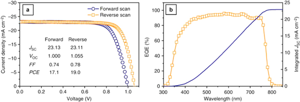
Figure 1. Device level characterizations. (a) Current density–voltage (J–V) curves in forward and reverse scan direction of a FTO/TiO2/MAPbI3–xBrx/Spiro-OMeTAD/Au device. (b) Corresponding external quantum efficiency (EQE) spectrum and integrated current density curve. Reprinted with permission from [24]. 2016 Nature Publishing Group Copyright.
Download figure:
Standard image High-resolution imageSeveral reports have demonstrated significant reduction or elimination of the hysteresis effect by various strategies. For example, a universal KI doping approach was demonstrated to be successful for FAMAPbI2.55Br0.45, FAMACsPbI2.7Br0.3, MAPbI3, and FAPbI3 perovskites and was explained by reduced bulk trap density and low-frequency capacitance [40]. Similarly, impurity phase management via incorporation of RbI was shown to improve charge carrier mobility and lifetime, as well as to suppress hysteresis in RbMAFA lead halide perovskites [41]. A different approach, namely realization of nearly ideal energy level alignment of the hole transport layer, eliminated hysteresis in MAPbI3 solar cells completely and was reasoned to be related to diminished interfacial charge accumulation [34]. Also, the passivation of surface trap states and/or states along grain boundaries via fullerene deposition represents a promising route to fabricate hysteresis-free MAPbI3 devices [35]. These findings point towards ion motion being a key contributing factor. In the absence of grain boundaries, ion motion is mediated by vacancies. To which extent the organic cation is mobile is currently under investigation. It is crucial to consider that these device level characteristics are determined using structures on the mm2 to cm2 scale. They reveal, however, properties of driven point defect heterogeneities down to the nm scale. While such processes are implied by these measurements, understanding the underlying mechanisms requires more advanced characterization.
Deeper device analysis to illuminate performance limitations include temperature-dependent and light-intensity-dependent J–V [19, 42, 43], admittance spectroscopy (AS) [44, 45–47], and sub-bandgap EQE [29, 48]. These approaches are widely used in semiconductor research and will be briefly discussed next.
Temperature-dependent and light-intensity-dependent J–V characterizations not only provide device efficiency trends under various operational conditions but also insights into loss mechanisms [49]. Temperature-dependent hysteresis effects suggest that multiple charging–discharging processes are responsible for the previously described hysteresis [50]. Tress et al reported on a comprehensive study using temperature-dependent and light-intensity-dependent J–V characterization on state-of-art mixed ion (CsMAFAPb(I0.83Br0.17)3) perovskite devices (figure 2(a)) to distinguish the dominant recombination loss mechanisms using different device architectures. In brief, it was found that optimized devices with Voc ∼ 1.2 V exhibit ideality factors (nID) ∼1.6 and Ea = Eg (with Ea being the activation energy of recombination and Eg the bandgap energy, respectively) which indicates recombination is dominant in the bulk absorber [19]. This conclusion is surprising due to findings discussed below (section: Nanoscale absorber level characterization) where significant numbers of surface defects with inhomogeneous lateral distribution have been observed by photoluminescence spectroscopy and shown to be healed by surface passivation. Thus, it is speculated that devices characterized by Tress et al might have had nearly ideal contact formation.

Figure 2. Device level characterizations. (a) Temperature dependent VOC of a FTO/SnO2/CsMAFAPb(I0.83Br0.17)3/ Spiro-OMeTAD/Au device at different light intensities. (b) Defect energy distribution of a perovskite device after energy conversion from capacitance–voltage (C–V) measurements at different temperatures. (c) Sub-bandgap EQE spectra for MAPbI3–xBrx perovskite devices with x = 0, 0.4, and 1. Fits to the data are shown as solid gray lines, with the underlying Gaussian defect distributions shown as solid blue and magenta lines. (a)–(c) reprinted with permission from [19, 44, 48]. 2017 Royal Society of Chemistry (a), 2015 Royal Society of Chemistry (b), and 2017 American Chemical Society (c).
Download figure:
Standard image High-resolution imageAS measurements provide another piece of the puzzle by investigating the concentration of defects and their energetic positions. These defect properties can be correlated with their device parameters and used to guide processes and materials towards high performance devices. The AS measurement utilizes the capacitance responses from the charging and discharging of defect states by modulating the bias voltage to extract the spatial charge distribution. This measurement yields the activation energy of the major defect state (Ed) and the defect distribution density within the bandgap, as illustrated in figure 2(b) (measured at different temperatures). The major defect states observed in FTO/TiO2/MAPbI3/Spiro-OMeTAD/Au devices include a major shallow-defect peak at 0.167 eV and a deep-level defect higher than 0.3 eV above the valence band [44]. The integrated densities of the major defect states in both cases are ∼1016 cm−3, which lie within the broad range of later reports, where values of ∼1015 to 1017 cm−3 were found [45, 46, 51, 52]. AS measurements sample an ensemble and are limited by assumptions about system homogeneity that can mask nanoscale heterogeneity. More specifically, the defect positions relative to the band edges are based on the assumption of the majority charge carrier type of the material, whereas doping in perovskites is poorly controlled.
The presence of defects has also been found by sub-bandgap EQE measurements (figure 2(c)) [48]. The response in sub-bandgap EQE measurements corresponds to transitions from bound to free electronic states that generate the photocurrent. Similar to AS, the sub-bandgap EQE measurement does not directly indicate whether the observed transitions are caused by trapped holes or electrons that are excited to the valence or conduction band, respectively. The energetic position of the sub-bandgap defect spectrum in FTO/TiO2/MAPbI3/Spiro-OMeTAD/Au devices was observed around ∼1.36 eV, which is ∼0.2 eV away from the band edge and consistent with the results from AS measurements [48]. Sub-bandgap EQE on mixed I/(I + Br) perovskites revealed the presence of a second defect extending into the bandgap that could explain the observed voltage losses in pure Br MAPbBr3 devices [48]. This finding suggests the presence of deep defects in mixed I/(I + Br) perovskites and ties back to low photoluminescence quantum yields (PLQYs) in MAPbBr3 as discussed later. Other defect states have been reported for FTO/TiO2/MAPbI3/Spiro-OMeTAD/Au with a deep-level defect state at 0.76 eV by Miller et al, which might be related to specific device preparation conditions and device quality [29]. By combining sub-bandgap EQE measurements with transient photocapacitance spectroscopy they found that such a deep-level defect may be present at the interface or originates from outside the perovskite layer [29]. In general, there appear to be frequent discrepancies in the detection and assignment of defect levels in halide perovskite materials that possess nominally identical composition. This gap likely points towards the importance of synthesis conditions in defining defect concentrations and distributions, but a systematic investigation does not yet exist.
It is important to note that there is clear evidence for a reduction in bulk and surface defect density when combining multiple cations in halide perovskites with decreasing defect density from MAFA > CsMAFA > RbCsMAFA [53]. An outstandingly high Voc of 1.24 V in a quadruple cation perovskite device (FTO/compact-TiO2/mesoporous-TiO2/RbCsMAFAPb(I1–xBrx)3/Spiro-OMeTAD/Au) with Eg = 1.63 eV was attributed to a major suppression of non-radiative recombination sources and reduced defect density [53]. Cation engineering was recently reported to heal deep defects in wide bandgap CsMAFAPbI3–xBrx (x = 0.25 and 0.4) compounds [54]. Using density functional theory (DFT) calculations this was attributed to the presence and reorientation of the dipolar MA cation which led to the absence of a second, deeper trap level [54]. Interestingly, this work stated that incorporation of MA might not reduce the formation of defects but rather leads to a passivation of deep defects. It is possible that such self-healing mechanisms are related to findings by theorists pointing out that perovskites are electrically benign and highly defect tolerant [5, 55]. As new compositions are explored, additional internal self-passivation processes may be discovered and it will be important to examine mechanisms by which they occur, especially with respect to mixed cation systems, in order to rationally optimize materials.
Macroscale absorber level characterization
Following the principle of detailed balance, if one considers a solar cell device at open circuit, where no current is flowing, all photons with hν > Eg are absorbed and create electron–hole pairs whose lifetimes are finite, i.e. they must ultimately recombine. In order to reach the Shockley–Queisser (SQ) limit the only recombination mechanism should be radiative [56]. In this regard, PLQY measurements are a powerful method to assess the relationship between radiative and nonradiative recombination. The dependence of the external (measured) PLQY on the illumination density for mixed halide MAPbI3–xBrx perovskites is shown in figure 3(a) [57]. Given the fact that ionic movement in the perovskite can result in inhomogeneities that change in space and time under non-equilibrium conditions, it is important to note that these PLQY measurements were performed without light soaking and before the appearance of any halide segregation (that is illumination induced demixing of I–Br compositions to form I-rich and Br-rich domains). The external PLQY first increases with increasing pump-power density, before it then reaches a plateau and eventually decreases at the highest pump-power densities used in this study due to dominant Auger recombination. The rise in PLQY at low excitation intensity has been observed by multiple groups for metal halide perovskites [57–60] and has been explained, in conventional manner, by gradual filling of trap states at low excitation until radiative recombination dominates when the trap states are filled [58, 60]. MAPbBr3 shows a significantly lower PLQY compared with MAPbI3 or mixed I/(I + Br) compositions. This finding can be related to the sub-bandgap EQE findings, where deep level defects were observed for pure MAPbBr3 [48]. Although perovskites are predicted to be defect tolerant, the PLQY measurements reveal considerable losses and illustrate that metal halide perovskites are limited by nonradiative SRH recombination at low excitation intensity, including 1-sun [57, 60, 61].

Figure 3. Macroscale absorber level characterizations. (a) External photoluminescence quantum yield of MAPbI3–xBrx films as a function of injected carrier density. (b) Internal PLQY of MAPbI3 films recorded over time under constant illumination in dry N2, dry air, and humid air. (c) Optically implied Voc in comparison to electrically reported Voc of various metal halide perovskite compositions: MA = CH3NH3+, FA = CH(NH2)2+. (a) Adapted with data previously published in [62]. (b) Reprinted with permission from [62]. Copyright 2017 Elsevier Inc. (c) prepared from data published in [53, 57, 69, 72, 104, 105].
Download figure:
Standard image High-resolution imageIt is crucial to recognize that unique properties of metal halide perovskites, such as light-induced ion migration and halide segregation, surface reactivity with the environment, and the co-presence of PbI2 phase, can significantly affect PL emission intensities. As an example, the atmospheric condition under which the PLQY is recorded plays a critical role [62, 63]. Brenes et al, showed a substantial improvement in humid air versus dry N2 or dry air, reaching internal PLQY values close to 90% [62]. Here, the internal PLQY is calculated from the measured external PLQY following the approach introduced by Richter et al [64]. Correspondingly, the minority carrier lifetime significantly increased, as depicted in the inset of figure 3(b) [62]. To explain the improvements in humid air, it has been proposed that the photo-induced reduction of O2 to O2– shifts shallow defect levels into the valance band, thus eliminating shallow defect levels [62]. These observations tie back to the role of the synthesis atmosphere, the reaction of the material with atmosphere, and how it could be employed to tailor better device performance and stability.
As a consequence of optical reciprocity, quantitative photoluminescence can serve as an invaluable measurement to derive one of the key parameters of a solar cell device, the open-circuit voltage (Voc) [65–68]:  where q is the elementary charge,
  the splitting of the quasi Fermi energies, and
  with
with  being the Voc in the SQ limit in which only interband radiative recombination occurs [56], Jsc the short circuit current density, and J0 the saturation current density. As mentioned above, any nonradiative recombination loss will lead to a voltage drop, and thus a loss of efficiency in a PV device. In the ideal case, the external PLQY (which is a number ≤1) is 1 and thus
The optically extracted (implied) Voc serves as an upper limit for the maximum achievable Voc purely based on the intrinsic material properties in the absence of effects associated with non-ideal selective contacts or subsequent processing steps that could lead to enhanced nonradiative recombination losses. Figure 3(c) summarizes the implied Voc values for MAPbI3–xBrx and FACsPbI3–xBrx perovskites calculated for the highest external PLQY measured, as well as for the PLQY at 1-sun (i.e., the PLQY obtained from intensity-dependent PLQY measurements [57, 69]). These are compared to the electrical Voc values reported for solar cell devices as a function of the absorber bandgap for different perovskite compositions including multi-cation and mixed 2D–3D perovskites. The clear discrepancy between implied and electrically measured Voc illustrates nonradiative losses at the contacts and was also pointed out in [61]. Together with PL measurements discussed before, as well as the device analysis by Tress et al, it appears that there are important losses in both the absorber itself and at its interfaces. It is known that wider bandgap mixed I/(I + Br) compositions (particularly MA-perovskites) show photo-induced halide demixing, which limits the device Voc as can be seen in figure 3(c) between ∼1.7 eV < Eg < 2.2 eV [70]. Interestingly, this halide demixing is significantly mitigated in mixed cation perovskites [11, 69, 71]. Mechanisms proposed to reduce this photo-induced effect include mixed halide phase stabilization via build-up of strain [69] and removal of halide vacancies in combination with immobilization of excess halides via electrically benign potassium-halide species that accumulate at grain boundaries and surfaces [11]. The exact mechanisms are still under investigation, with leading hypotheses based on strain affecting thermodynamics or vacancy concentrations primarily impacting kinetics. These are fundamentally different, though not necessarily mutually exclusive, mechanisms that involve complex interactions at the nanoscale. Improved understanding of the underlying processes will be important for designing stable absorbers with engineered bandgaps, which will be aided by probing these processes at their natural scales, as discussed below.
Another way to increase the bandgap is by interrupting the 3D perovskite structure by insertion of bulky cations, which form 2D structures (e.g. phenylethylammonium). These mixed 2D–3D perovskites clearly outperform their 3D counterparts with equivalent bandgaps and reach high device Voc values (green circles in figure 3(c)) [72]. One hypothesis is that interruption of the 3D crystal by 2D layers provides a way to limit ionic movement and, thus, induced heterogeneity. On the other hand, hysteresis is observed in both 3D and 2D perovskite solar cells, indicating that the underlying mechanisms causing hysteresis exist in both, even though ionic transport should be significantly limited in vertically aligned 2D perovskite devices [73]. 2D–3D perovskites are also used as passivating layers, e.g. on bulk FAMAPbI2.55Br0.45 films, and have been found to enhance stability as well as power conversion efficiency [74]. The proposed mechanisms are deactivation of surface traps and reduction of ionic movement via an interfacial energetic barrier [74]. Given these beneficial effects we anticipate more and more research with focus in this direction.
Overall, quantitative photoluminescence measurements provide a bridge between material properties of the absorber and the characteristics of devices. In particular, they reveal limitations of the absorber due to nonradiative recombination via defects, especially at low illumination densities, and recombination at selective contact interfaces. Similarly, PL can detect photo-induced halide demixing in mixed I/(I + Br) perovskites, which is reflected in changing spectral emission due to formation of I- and Br-rich domains under illumination. Such halide segregation leads to a much lower Voc relative to the bandgap of the mixed I/(I + Br) compounds. Thus, PL is a powerful method for connecting different length scales.
To this point, we have not addressed electronic transport properties (such as minority carrier lifetime  diffusion length
  and mobility
  linked via L =
  with the Boltzmann constant k, the absolute temperature T, and the elementary charge q) that determine function (e.g. Voc and Jsc). Considerable research has been devoted to understanding these parameters using a wide range of different methods. For example, mobilities have been determined by transient and steady-state methods such as time of flight (ToF), time-resolved microwave conductivity, Hall effect measurements, or THz spectroscopy [75]. Reported values vary by about 2–3 orders of magnitude (e.g. <1–70 cm2 V−1 s−1 reported for MAPbI3) [75, 76]. However, it is worth mentioning that the different techniques sample 'different mobilities' because of the different length scales that are probed—from the very local all-optical methods to the macroscopic long-range electrical methods—and 'different carriers' under illumination or in darkness. By comparing values obtained from methods that naturally probe interactions over very different length scales (i.e. THz versus ToF), it is possible to gain improved insight on how different factors, such as electronic structure, electron–phonon interactions, grain boundaries, and interfaces, impact charge transport, even if the methods themselves are not spatially resolved [75].
Nanoscale absorber level characterization
Exploiting the capabilities of advanced characterization techniques to resolve structural, optical and electrical properties at the nanoscale, it becomes evident that there are substantial heterogeneities in polycrystalline metal halide perovskite thin films that determine macroscale device performance metrics, transient characteristics, and synthetic reproducibility. In recent years, imaging or mapping techniques, including PL imaging [14, 15, 18, 62, 77], cathodoluminescence (CL) imaging [16, 78], atomic force microscopy (AFM) [17, 79], scanning micro x-ray diffraction (XRD) [14], electron beam-induced current [80], scanning near-field optical microscopy [77], Kelvin probe force microscopy (KPFM) [81–83], transmission electron microscopy (TEM) [14, 84], as well as non-laterally resolved techniques based on x-ray absorption spectroscopy [85–87], x-ray photoelectron spectroscopy [88], and solid-state nuclear magnetic resonance (NMR) spectroscopy [89–91] have been adopted to characterize local properties of metal halide perovskites.
Broad spatial distributions of PL intensity, significant grain-to-grain heterogeneities, and spectral emission shifts have been reported for polycrystalline perovskite films. Draguta et al pointed out extreme spatial heterogeneities in recombination dynamics of MAPbI3 with some regions dominated by bimolecular radiative recombination while others show the signature of carrier trapping [15]. As a consequence, the PLQY also shows lateral variations (compare figure 4(a)) [15]. Ultimately, those spatially heterogeneous properties were found to extend over length scales larger than the crystalline domain sizes [15]. This is interesting because it raises the question of whether grain to grain variations or, rather, longer range heterogeneities that are decoupled from the grain structure are dominant in defining lateral variations in loss processes. In a different study on nonstoichiometric MAPbI3(Cl) a PL intensity drop of ∼65% has been observed at grain boundaries [18] (figure 4(b)). Additionally, Cl-rich regions in MAPbI3(Cl) were correlated with higher PL signal and a vapor pyridine treatment was found to heal weakly luminescent domains [18]. Recently, Braly et al, demonstrated a PLQY of >90% after n-trioctylphosphine oxide (TOPO) surface treatment of MAPbI3 [92]. TOPO acts as an electron donating molecule binding to the MAPbI3 surface and thereby reduces nonradiative recombination [92], an effect that has been observed with other Lewis bases as well [10]. Not surprisingly, the surfaces of metal halide perovskite films are critical to performance. Both, chemical surface treatment of the light absorber and addition of passivation layers to selective contacts lead to reduced interface defect concentrations and are getting more and more research attention. The fact that surface treatments make dark grains bright as measured by PL implies an inhomogeneous lateral distribution of surface states. The respective trap-state densities for bright versus dark PL regions vary starkly, from <1 × 1015 cm−3 to 9 × 1017 cm−3, respectively (figure 4(a)) [14, 15, 18]. A huge spread of defect densities for similar material compositions calls, in our opinion, for the need of better understanding of the influence of the synthesis parameters on local material properties and surface passivation. In this respect, not just ex situ nanoscale probes, but in situ spectroscopies and microscopies during synthesis and processing, have great potential to enhance understanding of synthesis-property relationships.

Figure 4. Nanoscale absorber level characterizations. (a) Trap density map (left) and corresponding external PLQY (right). (b) Confocal PL image highlighting a bright (red square) and dark region (blue circle). (c) CL images taken at accelerating voltages of 1.5 (left) and 5.0 kV (right) and the corresponding depth within which 75% of the energy is deposited. Please note the different intensity scales. (d) 〈220〉 diffraction peak q map with lines indicating paths d and e (left) and traces of the 〈220〉 diffraction peak taken along paths d and e (right). (e) Two-dimensional photocurrent map. Positions 'x' and 'y' are discussed in the text. (f) Room temperature bright-field TEM image of a MAPbI3 film. Blue circles depict stripe contrast in some of the grains. (a)–(f) reprinted with permission from [14–18, 84]. 2016 American Chemical Society (a), Copyright 2015 American Association for the Advancement of Science (b), 2015 American Chemical Society (c), permission received from the authors (d), 2016 American Chemical Society (e), 2017 Nature Publishing Group (f).
Download figure:
Standard image High-resolution image
High resolution CL microscopy, in which electron beam-induced luminescence is detected along with secondary electrons as a function of excitation position, provides detailed insights into spatial distributions of the luminescence yield correlated to morphology [16]. CL microscopy confirms high variability in luminescence and hence radiative versus nonradiative recombination rates from grain to grain [16]. Additionally, depth dependent information can be inferred by tuning the electron acceleration voltage to reveal distributions in surface and bulk trap density [16]. Figure 4(c) illustrates CL images of MAPbI3 films on FTO/TiO2 taken at accelerating voltages of 1.5 kV (left) and 5 kV (right). The corresponding depths where 75% of the energy is deposited are 25 and 100 nm, respectively. The highest CL fluctuation between grains has been observed at the film surface (i.e. high intensity contrast) which indicates very heterogeneous surface trap densities while the defect distribution in the bulk appears more homogeneous (figure 4(c)) [16]. This observation is consistent with findings from laterally resolved PL measurements on perovskite films without chemical surface passivation treatment (discussed above). A consideration to keep in mind here is that halide perovskites are soft materials which degrade under various circumstances and 'harsh' measurement conditions. High e-beam energy can alter the perovskite properties by causing defect formation and phase transformation [93]. It was found that the degree of damage not only depends on the cation (CsPbI3 is more resistant than MAPbI3 or FAPbI3) but also on the defect density of the perovskite material [93]. In addition, it was found that the electron beam can induce ion redistribution in MAPbI3 [94]. This means CL is a powerful technique but extreme care must be taken in avoiding beam damage and, thus, evolution of artifacts caused by the energy of the probe.
Not only spatially resolved luminescence-based measurements point towards variation in trap densities (laterally and spatially), a recent diffraction study by Jones et al for the first time revealed how the variation in trap states ties to local strain distributions associated with halide vacancies [14]. In this study, crystallinity investigated via scanning micro XRD revealed strain-related defects and the existence of local grain clusters [14]. Figure 4(d) depicts the local map of the peak scattering vector q of the 〈220〉 diffraction peak (left) and selected slices (paths d+e) through the map (right). Using a first principles atomic model it was shown that introduction of compressive strain (using the relative shift of the q value) increases the concentration of charged iodide vacancies by a factor of 2 compared to the unstrained crystal [14]. It appears that the soft nature of the perovskite lattice is prone to local lattice contraction caused by a defect [14]. Distinct local patterns were found as evidence for regions with similar crystallographic properties called super-grains due to their dimensions being more than 10× larger than individual grains [14]. This is even more extreme in triple cation MAFACsPbI3–xBrx perovskites with super-grains being more than 1000× larger than single grains [14]. Jones et al suggest, that the super-grain size is the critical size that can be correlated to device performance and not the grain size extracted from SEM images [14]. In agreement and confirmed with PL mapping, spatially heterogeneous properties were found to extend over length scales larger than the crystalline domain sizes [15]. These findings not only link optical and structural properties on different length scales but also raise questions of, what is the origin of super-grains and how do they influence the overall device performance, is it grain to grain variation or, rather, longer range heterogeneities that are decoupled from the grain structure that define lateral variations in loss processes?
Photoconductive AFM on partial solar cell device stacks (e.g. FTO/TiO2/perovskite) is a powerful technique to directly link grain-to-grain and intra grain heterogeneities to device metrics, such as short-circuit current (Isc), Voc, and FF [17, 79]. For example, Kutes et al mapped the local photovoltaic performance parameters of solution processed MAPbI3-based half devices with nanoscale resolution [17]. This work illustrated interconnected aggregates of super-grain structures exhibiting similar magnitude of Isc and heterogeneous transport between interconnected grains and grain boundaries (figure 4(e)) [17]. The 'x' marker in figure 4(e) illustrates a grain boundary with enhanced Isc while the 'y' marker depicts a region (yellow) with lower Isc within an area of similar topography (red). Thus, topography-related artifacts are negligible in this case [17]. In a different study on MAPbI3–xClx (synthesized via a two-step vapor-assisted solution process [95]) Leblebici et al, found facet-dependent Voc and Isc variations within single grains indicative of facet-dependent defect concentrations [79]. These studies highlight that scanning probe methods are well suited to characterizing nanoscale heterogeneities in perovskite absorber layers and on their surfaces. Such studies allow for determination of connections between morphology and electrical transport properties. However, the requirement for physical interaction between the probe tip and the material itself makes it difficult to characterize buried solid/solid interfaces that are responsible for selective charge extraction. To overcome this limitation, researchers have applied scanning probe methods such as KPFM to device cross sections [81]. Bergmann et al revealed internal electrical potential distributions across the functional layers of a perovskite solar cell by real-space KPFM analysis [81]. It was found that excess holes accumulate in front of the hole selective contact under illumination and thus form an electrical barrier that limits the Isc [81].
Next, intra grain heterogeneity down to the 10 × 10 nm2 scale has been reported using high-resolution TEM [14, 84]. It appears that grains as they are viewed in the SEM are composed of many sub-crystallites with sizes between ∼10 and 100 nm [14]. Additionally, the presence of twin domains in tetragonal MAPbI3 was discussed by Rothmann et al and is shown in figure 4(f) [84]. Twin boundaries impact charge separation, transport, and recombination [96]. The width of the twin domains present in MAPbI3 films range from 100 to 300 nm and their formation/disappearance is reversible when transitioning through the cubic/tetragonal phase change [84]. This finding might have several implications on device operation because the operation condition of a solar cell spans the perovskite (MAPbI3) tetragonal-to-cubic phase transition temperature of ∼54 °C [97]. Synthesis of metal halide perovskites typically involves reaction temperatures around 100 °C followed by cooling to room temperature implying a transition from the high symmetry cubic phase to the lower symmetry tetragonal phase. It has been found that crystal twinning is related to this phase transition, possibly as a consequence of releasing internal strain [84]. It would be interesting to do the same study for MAPbBr3, which does not undergo a phase transition at these temperatures and compare the twin densities between the pure I versus Br composition. Furthermore, the appearance of striped domains (blue circles in figure 4(f)) with the same orientation before and after heating ('memory effect') may be driven by certain constraints such as strain or high defect densities [84]. This observation is intimately linked to nanoscale heterogeneities and potentially device performance. Furthermore, it is an example where post-growth processing might have a more limited affect than otherwise assumed. If there is such a memory effect, then annealing the films to reduce twins may not be as effective as one might anticipate. Rather, one would need to address the underlying non-ideality that drives twin formation in specific locations, for example by varying and optimizing synthesis.
In addition to explicitly laterally-resolved methods described above, a variety of macroscopic techniques offer powerful potential to unravel chemical compositions and interactions down to the molecular scale. Advanced synchrotron based hard x-ray photoelectron spectroscopy has been used to investigate the near surface chemical environment of double, triple and quadruple cation perovskites [88]. Varying the photon energy allowed for chemical composition to be probed at different depths down to ∼11 and ∼18 nm [88]. Philippe et al found unreacted FAI at the surface of MAFA perovskites, as well as when adding Cs and/or Rb [88]. Rb seems to be mostly located towards the bulk of triple cation RbMAFA lead compositions while Cs can be found homogeneously distributed in CsMAFA lead perovskites [88]. On the other hand, the distribution of Cs and Rb in the quadruple cation perovskite material is rather homogeneous [88]. For molecular-scale compositional and structural information, the combination of synchrotron based x-ray absorption spectroscopy with first-principles DFT calculations has proven to be very powerful [85]. It is sensitive to the Pb-halide bond lengths, halide chemistry, and octahedral tilting [85]. Finally, solid-state NMR spectroscopy is a suitable technique to shed light on the microscopic composition of MAPb(I1–xBrx)3 [89] and mixed cation halide perovskites [90, 91]. It was recently shown that Rb and K are not incorporated into the perovskite lattice while Cs is incorporated into the lattice with up to 15% in CsFA lead halide perovskite [90]. This is very interesting because superior device performance and stability were reported for Rb and K containing multi-cation perovskites but leaves us with questions of where are these alkali metals located, in which form are they incorporated, and what is the mechanism that leads to improved device performance? In this respect, it is interesting to compare to chalcogenide thin film solar cell materials such as Cu(In, Ga)Se2, in which it is well known that the alkali metals Na and K play important roles for their optoelectronic properties. In chalcogenides these alkali metals preferentially accumulate along grain boundaries [98] and could induce ion exchange reactions [99]. This research direction is still active and it took many years until some of those findings were broadly accepted. Thus, there is precedent for the expectation that an increasingly active sub-field will evolve within the perovskite community that will focus on mechanistic understanding of the role of alkali metals.
Discussion and outlook
In summary, metal halide perovskites are extraordinary semiconductors and represent highly promising building blocks for optoelectronic devices. A variety of studies have revealed heterogeneities with respect to optoelectronic properties, morphology, local recombination, and transport. However, only a few studies have provided direct causation of local disorder and device performance. Using multiple probes at identical locations at the nanoscale would offer much needed insight into how specific structural and chemical non-idealities and non-uniformities influence optoelectronic properties. However, achieving this aim is not trivial since different methods have different sample requirements. Furthermore, the propensity of metal halide perovskites to transform under relatively mild external forces also means that experimental probes can dramatically alter the material. At the same time, a key goal is to characterize how perovskites transform in the presence of electric fields and illumination. Thus, in situ tracking of the evolution of perovskites in active devices represents a challenge but has been demonstrated recently employing interdigitated back-contacted substrates [96].
There are many approaches to synthesizing metal halide perovskites. While facile synthesis is an appealing feature of this materials class, it also means that there is wide variability in material quality, absolute composition, and structure. Indeed, most nanoscale studies were performed using 'homemade' precursors and according to evolved procedures that have not been rigorously optimized. This raises the question: how generalizable are the findings?
While characterization of isolated perovskite films allows basic material properties to be determined, strong interactions at interfaces can dramatically affect microscopic loss mechanisms and instabilities. In an active device, the perovskite absorber does not exist in isolation and the influence of selective contacts must also be considered. For example, to what degree can insights gained from films on quartz substrates, be applied to films that are located between TiO2 and spiro-OMeTAD? The presence of these contacting phases leads to electronic and chemical interactions, accumulation of charges, as well as local changes in structure, disorder, and morphology.
Most of the heterogeneities discussed above were investigated in MAPbI3 or MAPbI3–xClx perovskites. More recent multi-cation perovskites (e.g. KCsFAMAPbI3–xBrx) facilitate higher conversion efficiency and wider processing windows and synthesis protocols (as demonstrated for CsMAFA over MAFA [100] or RbCsFA over CsFA [101] compositions). Wider processing windows result in better reproducibility and is the prerequisite for a systematic study of synthesis conditions where uncontrolled variables such as glovebox history are not influencing final film properties. The chemically more complex materials have until now mostly been studied with a focus on device level impact (efficiency and stability) but only very few reports investigated the aspects of evolving/reduced heterogeneities in these multi-components. The intriguing findings of Cs being incorporated into the lattice while Rb and K are not, raise important questions regarding generalizable design rules. Comparison to Na/K-doped chalcogenides gives us a flavor on how distinctly those alkali metals could alter material properties. This leaves plenty of room for exciting new research avenues where composition-function relationships remain to be established. Similarly, 2D–3D perovskite compositions show enhanced device stability but, thus far, reports have mostly focused on device aspects with less attention to dedicated nanoscale characterization. Given the importance of such characterization approaches in advancing understanding of traditional perovskite compounds, such as MAPbI3, it is clear that focus will soon turn to heterogeneous nanoscale structural and optoelectronic properties in these systems. Such studies will be vital for addressing remaining knowledge gaps and for connecting our understanding with that of their 3D counterparts.
Future research will illuminate which nanoscale heterogeneities have to be eliminated to overcome efficiency loss and instabilities or can be exploit for new applications. A better understanding of mechanisms leading to efficiency increase and stability is needed to facilitate rational optimization of synthesis and composition. In a next level of sophistication, researchers should consider how to use that information to direct synthesis. If, for example, super-grains dominate and define local charge transport, how can their desirable properties be expanded over the full perovskite absorber? Potentially, there is a need for new synthesis routes with targeted growth of certain crystal orientation, controlled nucleation, and strain engineering. In this respect, one avenue here is the development of in situ probes to monitor synthesis while the compound is formed. A first step to such a comprehensive strategy to addressing synthesis-function relationships will require connections to be drawn between specific heterogeneities and their influence on macroscopic properties. To conclude, in our opinion there is a strong call for the application of complimentary nondestructive probes that can help to correlate the properties of local disorder with macroscopic function.
Acknowledgments
This manuscript was prepared with support from the Laboratory Directed Research and Development (LDRD) program of Lawrence Berkeley National Laboratory under US Department of Energy contract number DE-AC02-05CH11231 (T-BS and CMS-F) and by the Solar Photochemistry Program of the US Department of Energy, Office of Science, Office of Basic Energy Sciences, Division of Chemical, Geological and Biosciences under Contract No. DE-AC02-05CH11231 (CMS-F). IDS acknowledges TUM Solar in the context of the Bavarian Collaborative Research Project Solar Technologies Go Hybrid (SolTech).
Notes
The authors declare no competing financial interest.
Author contributions
The manuscript was written through contributions of all authors. All authors have given approval to the final version of the manuscript.