
Abstract
In this paper, an integrated microprism matrix for light coupling and optical sensing systems is presented. The matrix was fabricated by use of controlled negative pressure glass thermal reflow process by the use of monocrystalline mold. The single glass microprism had height of 250 µm or 350 µm with base width respectively 350 µm or 500 µm. The matrix was formed by 10 × 10 microprisms with distance between the microprisms from 150 µm to 400 µm. It corresponded to total area of the matrixes from 28 mm2 to 74 mm2. The controlled coupling of the beam into a substrate was obtained through determination of optimal geometric dimensions of microprisms and configuration of a measurement setup. Optimal position of the fluorescence induction light source in relation to the matrixes (0.5 cm to 4.5 cm distance, 30° angle of incidence) and microfluidic channel (4 mm) were determined. The fluorimetric tests (with excitation by 470 nm laser diode in all the experiments) carried out using fluorescein solution, microbeads and porcine oocyte indicated the possibility of using a microprism matrix for fluorimetric image-based 500 nm long-pass detection in lab-on-a-chip platforms.
Export citation and abstract BibTeX RIS

Original content from this work may be used under the terms of the Creative Commons Attribution 4.0 license. Any further distribution of this work must maintain attribution to the author(s) and the title of the work, journal citation and DOI.
1. Introduction
Lab-on-a-chip platforms have the potential to create integrated, miniaturized and standalone laboratories, on which the different instrumentations and functionalities of biological and chemical laboratories may be applied. Lab-on-a-chip platforms present opportunities to reduce manual handling for sample processing and limit the requirements for highly trained staff. Typical dimensions of microfluidic chips range from millimeters to few centimeters. The small size of the lab-chip reduces the amounts of required reagents, solvents and biological samples, which also reduces overall costs and time for analysis. The efficiency of microfluidic-based methods can be much higher than conventional laboratory methods due to the possibilities of controlling and manipulating fluids and gases along with biological matter (e.g. cells, microorganisms) within microfluidic structures [1–3]. However, lab-on-a-chip devices still need a macroscale, often bulk, measurement setup that is not very compatible with microfluidic devices. The instrumentation is often standard laboratory equipment, which is used due to the lack of alternatives to conventional laboratory methods and instrumentation in biological and chemical procedures that usually accompany measurements. In such situations the benefits of miniaturization of microfluidic devices are lost, and advantages obtained through the application of Micro-Electro-Mechanical System (MEMS) technology are overshadowed by problems arising from the need to use detection systems, imaging instruments such as microscopes, and other large-scale functional components such as fluid and gas controllers, or micromanipulators [4–6]. A large part of the lab-chip instrumentation is optical components and systems, due to the popularity of optical detection methods and microscope-based imaging techniques in biological and chemical research.
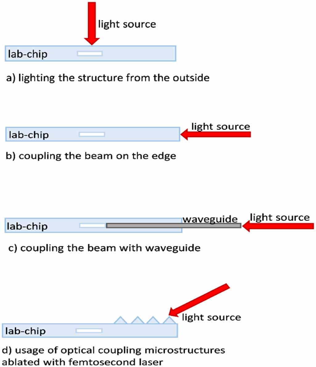
One of the most challenging setbacks is often the complex optical alignment of macro-scale infrastructure to microfluidic chips, along with coupling the light beam into the micron-sized detection area within the microfluidic system [7]. There are several methods of light coupling into the microfluidic structure of a chip (figure 1). In a setup where light is illuminated onto the surface of the chip, conventional optical elements such as band-pass filters, microscope lens, mirrors and microscope objectives are used to focus the light beam within the detection area of the chip (figure 1(a)). The light beam that interacts with the sample propagates in air on the other side of the chip to the detection system. To align all appliances with the detection area precise translation stages are commonly used [8].
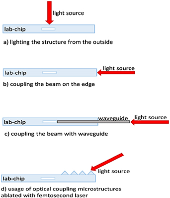
Figure 1. Main methods of beam coupling in the microfluidic system.
Download figure:
Standard image High-resolution imageAlternatively, the area of light coupling can be on the edge of the substrate, assuming that the microchannel network is not complex, and the detection area is placed near the edge of the chip [9] (figure 1(b)). This setup is usually used for fluorimetric measurements, where the detector is placed at an angle of 90° to the light illumination on the sample [10, 11].
In order to bypass the substrate separating the light beam from the tested sample, waveguides are used to provide the beam directly to the detection area (figure 1(c)). In this method it is necessary to incorporate additional fabrication steps to obtain grooves for optical fiber alignment. This solution also has some limitations—such as optical fibers incorporated into the substrate taking up space and forcing the use of simpler microfluidic paths [12–14]. There are solutions in which the core of the waveguide or both core and cladding are made of liquid and assembled within the lab-chip. In cases where only the core is liquid, cladding is usually made of material film deposition within the etched grooves or microchannels. The light is then transmitted within an integral part of the lab-chip, in a way that the sample is transported with fluids or gases [15]. In liquid-liquid configurations laser light is guided by the fluidic waveguide, which is generated by an interface between two liquids with different refractive indices but similar density [16].
The last method for coupling light from the outside of the chip is by fabricating microstructures such as lenses or prisms onto the lab-chip (figure 1(d)).
Comprehensive review of integrated micro-optics for microfluidic analytical applications was presented recently by H. Yan and M Gijs [2]. Generally the microprism exploit the material properties to manipulate the power and direction of traveling light waves. The integrated microprism are made of Polydimethylsiloxane (PDMS) or Poly(methyl methacrylate (PMMA) and work as micromirror, tunable angle deviation microdevice or component of total internal reflection circuit [2]. Individual glass miniature prism, assembled to the chip after PDMS-glass structure fabrication, was successfully applied as mirror in light-sheet microscopy [17]. In case of light coupling the microprisms enabled seamless integration with printed circuit boards and permit the optical elements to be located off-chip without use of epoxies or adhesives [17].
Often coupling microstructures are ablated with femtosecond laser or hot embossed in glass or molded in a layer of polymer on top of the chip [18–22]. Usage of each kind of material for lab-chip and microstructures fabrication brings limitation either for biological analysis possibilities or optical detection efficiency. In general, polymer (including PDMS or 3D printing [23]) optical microstructures are easier and quicker to fabricate than glass structures. On the other hand, fabricating lab-chip in polymer material brings more limitations in case of performing biological experiments such as biocompatibility issues, resistance to chemical reagents or swelling of the polymer such as PDMS. Hybrid lab chip systems with polymer optical structures and glass microfluidic channels creates additional transition of laser beam from one medium to another producing additional beam scattering. In terms of optical properties, chemical resistance and biocompatibility glass seems to be the best choice so far. However, it should be noted that the integration of optical and fluid structures is more difficult and time consuming in glass. Repeated use of structures compensates for these difficulties provided that the procedure for cleaning structures between experiments is relatively simple or automated. When it comes to optical microstructures in glass, fabrication processes involving glass molding technologies have been described in more detail in another publication [23]. Also glass thermal reflow process is used for fabrication of glass microlenses [24, 25]. Microprism fabricated by this technology was nor reported in the literature
The optical set up for light coupling is usually fixed during experiment and allows only for one detection area within lab-chip per specific alignment. Due to the bulky instrumentation, freedom in determining the path of beam propagation is lost. Similarly, by incorporating waveguides within lab-chip and providing laser beam directly to the detection area light propagation path is fixed. The use of several sets of light sources and detection systems in one chip to obtain more detection areas within one lab-chip is often impossible due to the bulky size of the individual components. Switching between detection areas using one optical system is also inefficient.
Ideally, experiments should be conducted in several areas within one lab-chip at the same time for better efficiency or let to the entire sequence of fluorescent tests to be carried out for different excitation wavelengths. Currently, the greatest potential to implement such a system have optical microstructures integrated with microfluidic structures [2]. They can be implemented anywhere on the surface of the lab-chip, and depending on the number of such structures or its arrays, they can be fabricated in many places at once. With specific shape of microstructure more than one light propagation path can be created using same optical structure. In case of square pyramid each side wall can be used to determine the propagation beam path to one of the four detection areas.
In this paper, an integrated microprism matrix for light coupling and optical sensing systems is presented. Glass reflow technology of glass microprisms matrix was developed and optimized. The controlled coupling of the light beam into a substrate was obtained through determination of an optimal geometric dimension of microprisms and configuration of a measurement setup. The fluorimetric tests carried out using a fluorescein solution, microbeads and porcine oocyte indicated the possibility of using the matrix of prisms for fluorimetric detection in lab-on-a-chip platforms.
2. Design and fabrication
The fabrication of glass microprisms was based on a five-step process (figure 2(a)). First, silicon replica was formed by selective etching in KOH solution. The replica was etched in a (100)-oriented monocrystalline silicon substrate where a square pattern was aligned in the <110> direction. The side walls of the etched pyramid were defined with a (111) plane with a 54.7° angle in relation to the (100) plane. The vials were etched in 40% KOH at 80 °C. To create precise cavities in the shape of inverted normal pyramids, the so-called vials, the geometry of the patterns on the mask was precisely designed. The height of the pyramid was limited by the thickness of the silicon substrate. To obtain pyramid with its side wall area bigger that laser spot size (in this case at least 5 mm in diameter), the pyramid should have height equal to about 6 mm. Using silicon substrate with the thickness of 6 mm is far too expensive to fabricate such microstructure. Moreover, taking into account that overall thickness of microfluidic chip is 2 mm, adding 6 mm of height to the structure decreases the advantages of miniaturization. Instead, array of smaller pyramids was designed to obtain the largest possible total surface area of the side walls of the prisms when using the smallest possible array surface.
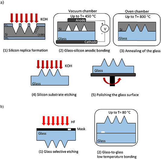
Figure 2. Scheme of microprism fabrication process: (a) step-by-step process, (b) integration with microfluidic channel.
Download figure:
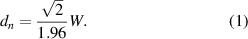
Standard image High-resolution imageThe mask with square windows was chosen to meet the formula (1), where W is mask width and dn is the groove depth. Due to the thickness of the silicon substrate (380 µm ± 20 µm), the pyramid height was limited to around 350 µm. On the other hand, in order to obtain the largest possible surface area of the pyramid side walls, the pyramid height was not less than 250 µm.
Next, the silicon substrate with replica microprisms was anodically bonded with the glass substrate (Borofloat 3.3, Schott) in a vacuum (∼10−3 mbar) and in high temperature (∼450 °C) and voltage (∼1 kV), thus low pressure remained in the pyramid cavities. The pressure difference between atmospheric pressure outside the cavities and low pressure inside the cavities, at annealing temperature (step 3) caused glass 'collapsing' and filling of the cavities. The appropriate glass microprisms were then formed under the effect of annealing in the oven up to 800 °C. Optical microstructures were revealed by complete etching of silicon substrate in KOH solution (step 4). Finally, the glass surface on the other side of the microstructures was polished removing approximately 200 µm of material (step 5). After fabrication and geometry optimization of the microprism matrix, microstructures were integrated with the microfluidic channel in two steps (figure 2(b)). The microfluidic channel was etched through polymer tape working as a mask at a depth of 300 µm. After a cleaning procedure consisting of Piranha solution, for example, glass substrate with an integrated microchannel and microprism matrix was bonded with another glass substrate in the oven (up to 80 °C) for several hours. Applied here, low temperature glass-to-glass bonding was developed earlier and used elsewhere [26].
During the microprism fabrication process, and before optimization, several defects were observed. An uneven filling of replica with glass during annealing occurred when anoding bonding of replica and glass substrate was performed in too low a vacuum, and when a pocket of air was encapsulated between substrates within pyramids. After unsuccessful anodic bonding, the degree of glass filling during substrate annealing varied, and in the worst case did not fill the vials in the silicon at all (figure 3(a)). The generation of air bubbles was observed due to rapid temperature changes during the annealing process and fixed in the material in the vicinity of the contact of silicon with glass. Such defects eliminate microstructures from usage, mainly because they cause too much dispersion of light propagating through the glass or prevent coupling of the light into material in the first place. As a result, the temperature rise should be mild enough and spread across a few hours to obtain better control over the annealing process. The annealing time at a maximum temperature of 800 °C should last approximately 1 h.
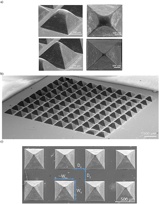
Figure 3. SEM photos of glass prism examples: (a) at the top partial structure, at the bottom almost whole structure (left images) side view (x22) and view from above (x130, right images), (b) the glass microprism matrix containing 100 glass pyramids (52.56 ± 0.03 mm2), SEM x22, (c) SEM photograph (x20) of prisms with geometrical parameters of the matrix: width of the prism base (Wx, Wy), and distance between the prism bases (Dx, Dy).
Download figure:
Standard image High-resolution imageDuring annealing when a temperature of ∼650 °C and higher is achieved, glass softens to the point that material starts to fill the cavities in silicon replica. During this process, the material liquefies in its entire volume, which can cause material spreading in places where it is not bonded to silicon. This can affect the later bonding of glass substrates, or in extreme cases disable it. Therefore, it is necessary to make sure that the substrate is arranged in parallel with an even surface during annealing, and if necessary, polish the glass surface after removing silicon in KOH solution.
As a result of technology optimization, a series of microprisms was fabricated, where due to the anisotropic structure of silicon each microstructure's side wall was inclined at an angle of 54.7°. The quality of the surfaces and edges, and also the repetitiveness of shape reproduction of the microstructures, were inspected with a scanning electron microscope (figure 3(b)).
After optimization of the fabrication processes glass microprism matrices with various geometrical configurations were prepared (table 1). The height of the microstructure and width of the base were taken into account. The general assumption was the bigger the surface of the side wall of the microstructure the better coupling of the light. Another dimension important for consideration was the distance between microstructures because of the possibility of the prisms shading each other during illumination.
Table 1. Various geometrical configurations of the glass microprism matrix (10 × 10 prisms in each matrix).
| Matrix | Height of the | Width of the prism | Distance between the | |
|---|---|---|---|---|
| configuration | prism (µm) | base Wx, Wy (µm) | prism bases Dx, Dy (µm) | Matrix area (mm2) |
| A | 350 ± 15 | 500 ± 10 | 250 ± 10 | 52.6 ± 0.03 |
| B | 300 ± 10 | 59.3 ± 0.03 | ||
| C | 350 ± 10 | 66.4 ± 0.03 | ||
| D | 400 ± 10 | 74 ± 0.03 | ||
| E | 250 ± 15 | 350 ± 10 | 150 ± 10 | 23.5 ± 0.03 |
| F | 200 ± 10 | 28.1 ± 0.03 | ||
| G | 250 ± 10 | 33.1 ± 0.03 | ||
| H | 300 ± 10 | 38.4 ± 0.03 |
As well as the prisms' height the following geometrical parameters were included: the width of the prism base (Wx, Wy ) and the distance between the prism bases (Dx, Dy ) (figure 3(c)). Before the final selection of the geometric parameters of prisms to be integrated with the microfluidic circuit structure, the structures were subjected to light coupling tests.
3. Measurement setups for optical characterization of the microprisms
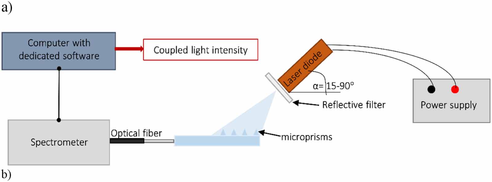
The first step was to define the optimal geometric dimensions of microprisms and matrices as a whole to obtain the best light coupling efficiency. In order to examine which dimensions were optimal, a series of tests was performed by measuring the intensity of the coupled laser beam propagating through the microprisms and then the glass structure to its edge. Tests were carried out for different angles (α) of incidence ranging from 15° to 90° (figure 4(a)).

Figure 4. Diagram of the measuring set-up for testing the quality of the laser beam coupling.
Download figure:
Standard image High-resolution imageA reflective filter with optical density 1.0 was placed after the laser diode with a wavelength of 635 nm. The light intensity was measured with spectrometer (OceanOptics USB 4000) equipped with optical fiber as a probe, using Spectra Suite software. The fiber was coupled to the 'output' edge of the glass substrate. After determining the optimal configuration of the coupling microstructures, a series of measurements was conducted to identify the most efficient arrangement of matrices and microfluidic detection area within the glass substrate. For this purpose, the optical power of the laser beam coupled within the glass structure was measured. In this measurement setup the spectrometer was replaced with a power meter (PM130D, Thorlabs). The laser diode (λ = 470 nm) was characterized by measuring the optical power depending on the current applied. In all subsequent measurements, the input optical power was set at 9 mW. The most important parameters taken into consideration were horizontal distance D1 between the detection area and the microprism matrix, and the vertical distance D2 between the laser diode and the glass structure, and optimal angle of incidence. This experiment allowed channel depth, distance between edge of the channel and microprism matrix, and size of the detection area of the microfluidic lab-chip to be selected.
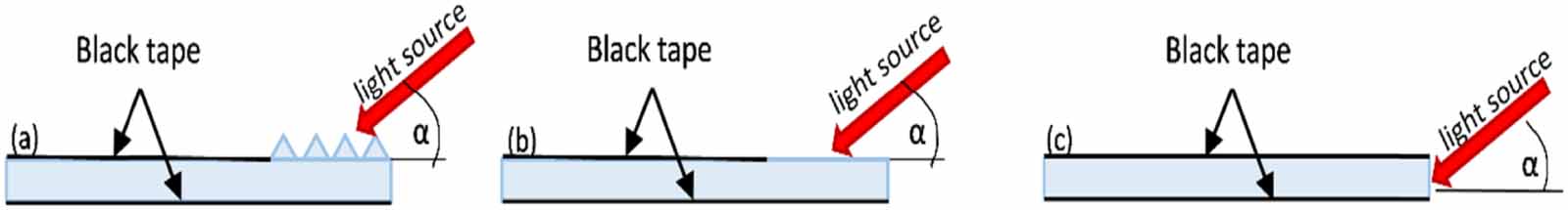
The reference measurements were also included to compare the effectiveness of light coupling within the glass using non-structurized substrate areas (figure 5) as well as the measurements with microprisms. Plain glass with a non-modified surface area and without the prism's matrix and edge coupled light were investigated. All parameters and setup configurations for this test remained the same. To complete the comparison, a beam was also coupled on the edge of the substrate, changing the angle of incidence from 15° to 90°. The surface area that was not illuminated was covered with black tape. In the experiments where the influence of D1 was investigated, the size of the spot illuminating the matrix was always the same (Ø = 8 mm). In the D2 experiment, the size of the spot varied with distance of D2 (from around 7–9 mm).
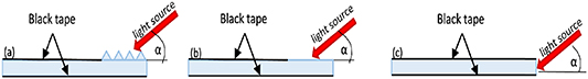
Figure 5. Reference methods of beam coupling in the microfluidic system: (a) using microprism matrix, (b) without coupling microstructures, (c) by the edge of the substrate.
Download figure:
Standard image High-resolution image4. Results and discussion
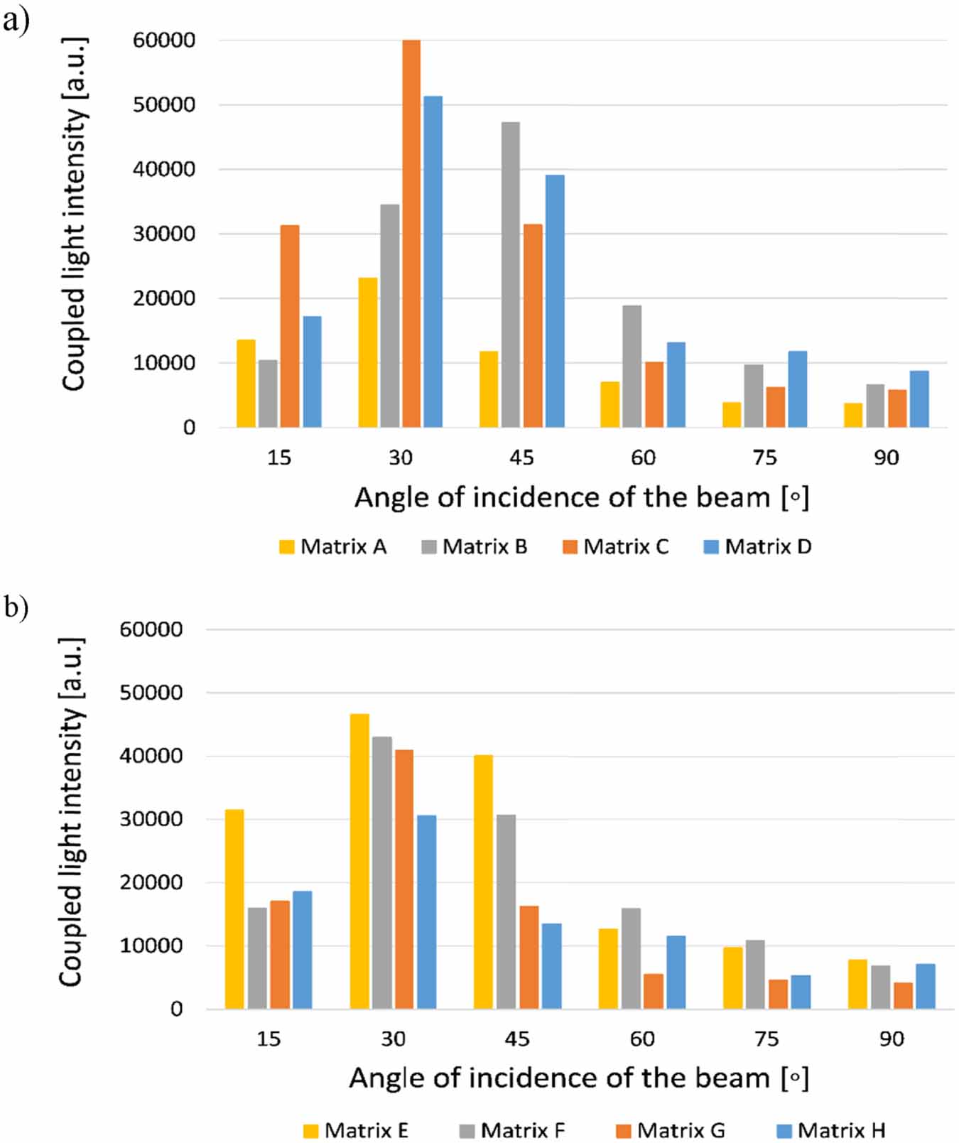
Each matrix configuration listed in table 1 was examined in terms of structure, surface quality and dimensional repeatability. The optimal geometric dimensions of microprisms and matrices as a whole were determined due to light intensity measurements of the coupled beam. The coupled light intensity depended on the angle of the beam indication, assuming that the laser beam spot always covers the entire matrix surface and does not go beyond its borders. The results show that the relationship between the width of the prism base and the distance between the prism bases affects the amount of coupled light (figure 6).
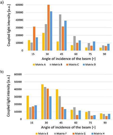
Figure 6. Dependence of the light beam intensity measured at the edges of the substrate for different angles of incidence (α) of the beam on the glass surface for various configurations of prism matrix: (a) for matrixes A to D (350 µm height), (b) for matrixes E to H (250 µm height).
Download figure:
Standard image High-resolution imageIt was found that geometric parameters significantly influenced coupling efficiency. If the prisms were too close to each other, then they covered each other, reducing the overall beam coupling surface of the matrix, whereas when microstructures were too far away, the surface of the glass was not used effectively, and most of the beam was scattered on the surface of the glass substrate and did not propagate within the material. The size of the microprisms also affected the results in a way that the larger the microstructure was, and therefore also the side wall area of the pyramid, the larger the coupling surface of the beam.
As a result, the optimal geometric dimensions of microprisms were defined and the matrix configuration labeled as C was chosen for the next measurements (table 2).
Table 2. Optimal incitation angle for each matrix configuration.
| Matrix | Coupling angle | Normalized |
|---|---|---|
| configuration | (max intensity) | intensity (max = 1) |
| A | 30 | 0.38 |
| B | 45 | 0.78 |
| C | 30 | 1 |
| D | 30 | 0.85 |
| E | 30 | 0.77 |
| F | 30 | 0.71 |
| G | 30 | 0.68 |
| h | 30 | 0.51 |
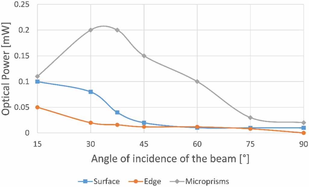
Using optimized prism matrices, reference measurements were conducted according to the methods shown in figure 5. Results show that the highest optical power was measured for the microprisms set up at around 30°–40° of incidence (figure 7).
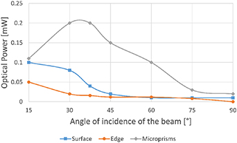
Figure 7. The dependence of the optical power of the coupled beam on the angle of indication for different laser beam coupling methods (matrix configuration C).
Download figure:
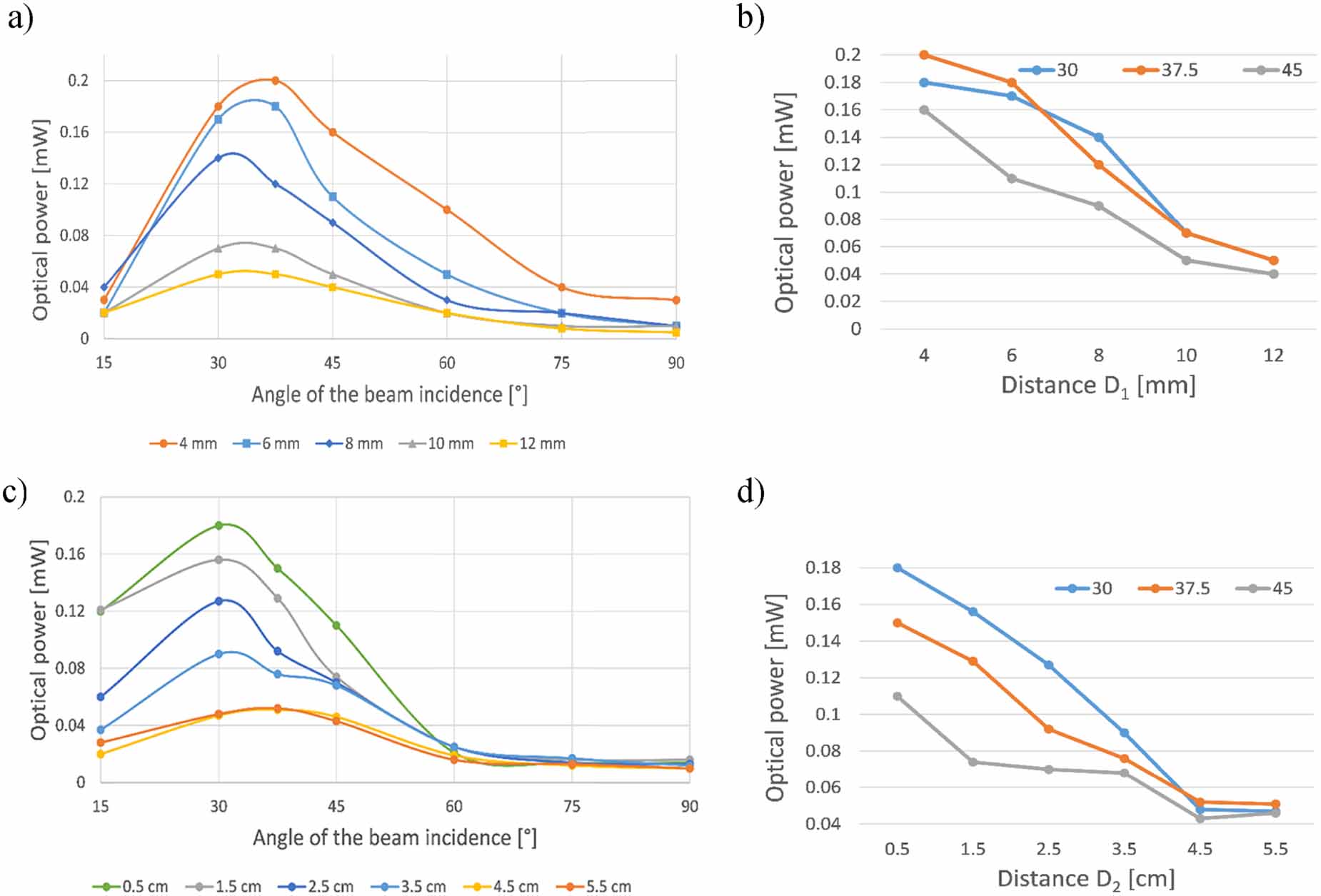
Standard image High-resolution imageThe most efficient arrangement of matrices and microfluidic detection areas within glass substrates were then studied. The distance between the laser diode and the coupling microstructure, both horizontal and vertical, combined with varying angles of incidence, influenced the value of optical power coupled to the glass (figure 8). The smaller the distance of the configuration of the prisms from the measured edge, the greater the optical power of the coupled beam. Also, the highest value of the optical power was obtained for 30°–37.5° of laser diode indication relative to the substrate, in every measurement.
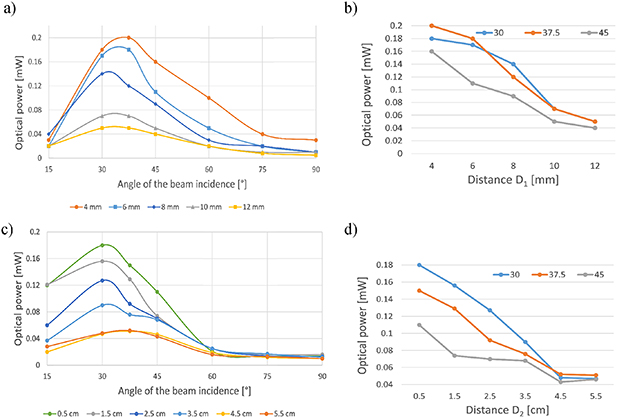
Figure 8. The dependence of the optical power of the coupled beam (a) on the distance of the configuration of the prisms from the measured edge (D1 from 4 to 12 mm), (b) on the incidence angle of the laser beam, (c) on the distance of the diode from the surface with prisms (D2 from 0.5–5.5 cm), and (d) on the incidence angle of the laser beam.
Download figure:
Standard image High-resolution imageAssuming that the whole matrix is illuminated in all the tests and the laser beam is divergent, an increase in D2 causes a decrease in the optical power density covering the matrix area. This can be eliminated by a coherent beam by adjusting the geometry of the laser light cone after changing D2.
Those results correspond to the geometric alignment of the laser light in relation to the side wall of the pyramids (figure 9). Considering that the pyramid's side wall is inclined at an angle α = 54.7°, the optimal angle β of light indentation would be 35.3° to obtain the right angle in relation to the side wall of microstructure (δ = 90°). Through coupling the laser beam with the angle β equal to 30°, an angle of indentation in relation to the side wall δ equal to 84.7° is obtained, which is the nearest value among the angles of coupling measured (15°–90° range). Investigation of the optimal distances of D1 and D2 showed that much of the light propagating through the glass was lost due to not fulfilling the condition for the total internal reflection (TIR) phenomenon [27]. Given that the refractive index of the borosilicate glass was 1.52 [28] for λ = 470 nm, the limiting angle for TIR was equal to 42°. In order to fulfill this requirement, the side wall of the pyramids α should be higher than 42°. Due to the fabrication possibilities of the silicon, this value was unattainable.
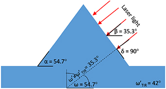
Figure 9. The schematic representation of the geometrical alignment of the laser light in relation to the side wall of the pyramids and TIR conditions.
Download figure:
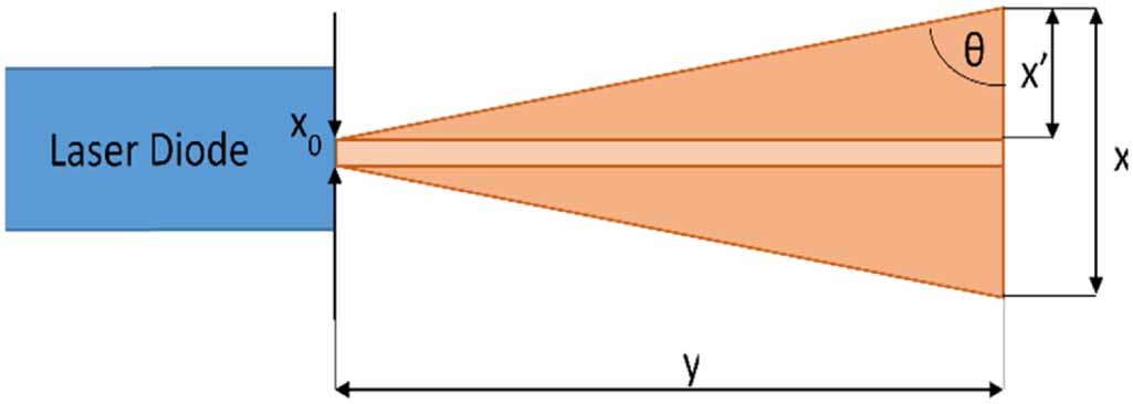
Standard image High-resolution imageApplied laser beam is divergent, therefore incident angle will depend on the position for each pyramid in relation to the position of light source (figure 10). The laser beam indentation angle θ to the surface may differ from right angle up to 10°–12°. According to the results of beam coupling investigation highest optical power was obtain for 30°–45° of the incidence angle which gives roughly up to 15° of the manipulation range.

Figure 10. Scheme of the impact of the divergent character of laser beam on the optimal incident angle of the beam with formulas necessary for laser beam indentation angle θ calculation.
Download figure:
Standard image High-resolution imageBased on the results obtained, the main conclusions arise from an optimal coupling angle, matrix configuration and dimensions, strong dependence of the light intensity in the glass on the distance from the microprism matrix and the dependence of the coupling light intensity on the distance between light source and the matrix.
The final measurement setup for further beam coupling investigation was determined as follows: 4 mm for the distance of the prisms to the microchannel, 30° for the angle of incidence and 4.5 cm for the distance of diode from the surface. For microfluidic chip configuration setup, but also for ease of usage during the measurements, the selected distance of the diode from the glass surface was higher than the distance determined as the best (here 0.5 cm).
5. Microfludic chip with integrated microprism matrix
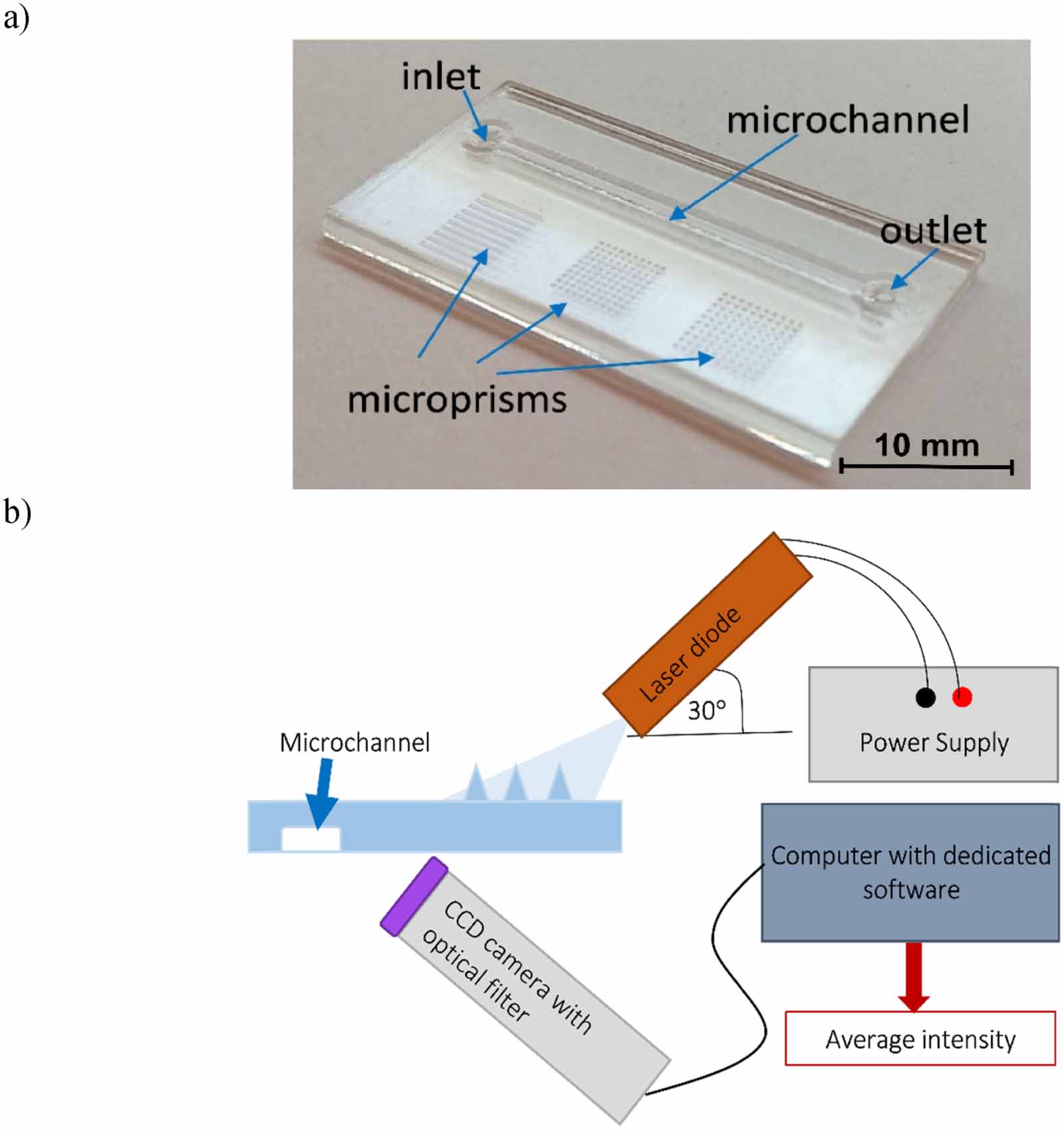
As a result, a microfluidic chip was obtained with a straight microchannel with a depth of 300 µm and multiple matrices on a single substrate (figure 11(a)).
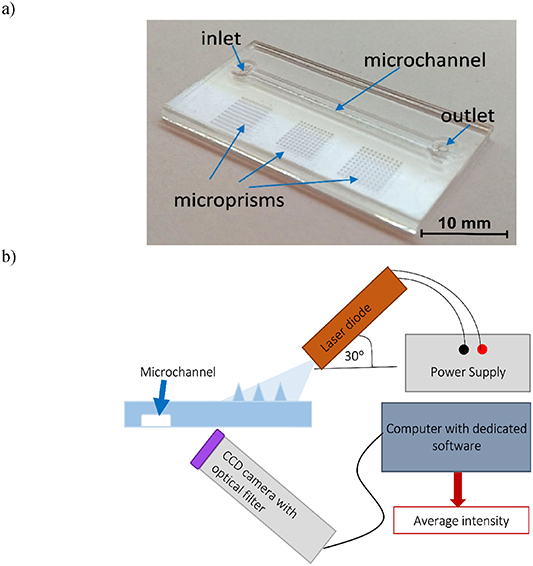
Figure 11. Photograph (a) of the microprisms integrated with microfluidic structure (microchannel: length 25 mm, width 1 mm, depth 300 µm) and (b) diagram of the measuring setup for fluorimetric detection tests.
Download figure:
Standard image High-resolution imageIn order to confirm that the optical power of coupled light is sufficient to perform fluorimetric excitation in a lab-chip platform using a microprism matrix, fluorimetric tests were conducted (figure 11(b)).
The detection area was observed with charge-coupled device (CCD) camera with an optical filter (long pass 500 nm). Debut Video Capture Software was used to capture pictures of the fluorimetric detection area and image analysis was performed using software developed in LabVIEW [10, 11].
For each photograph the average intensity of the pixels from the detection area was read. The volumetric fluorescence tests were carried out using a fluorescein solution with various concentrations ranging from 0.5 to 500 µg ml−1 (figure 12(a)) and a laser diode (λ = 470 nm) to excite the fluorescence. Additionally, fluorescence of the fluorescent red polyethylene microspheres (Cospheric) was observed in same measurement configuration (figure 12(b)). As a result, each microbead (about 70 µm in diameter) was clearly visible and distinguished in the microchannel. Also dye labeled porcine oocyte (about 110 µm in diameter) was well observed in the microfluidic channel. Therefore, the coupled optical power of the beam was sufficient to excite fluorescence in the microchannel for both volumetric and individual components (i.e. cells, oocytes, microbeads), even for non-optimal distance D2.

Figure 12. Tests of the fluorescence induction and measurements: (a) the dependence of the average intensity of the concentration of fluorescein in water (from 0 to 500 μg ml−1) with captured photographs at the microchannel for each concentration, b) photograph of the fluorescence of microbeads (left image) and porcine oocyte (φ = 110 µm, right image) in the microchannel.
Download figure:
Standard image High-resolution image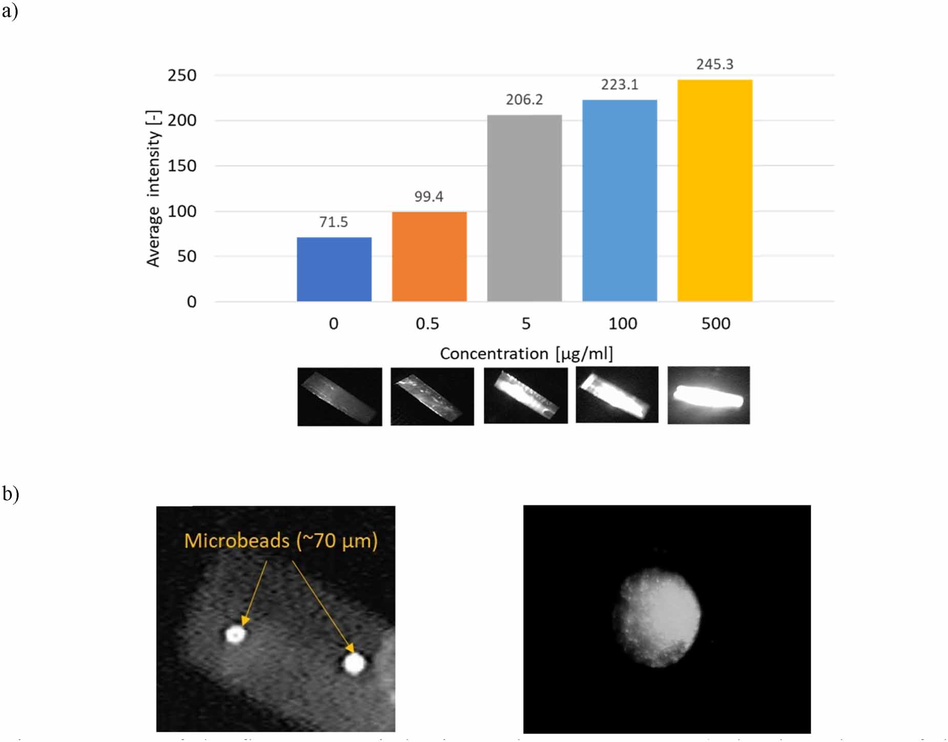
The coupling efficiency at level of several percent might seem low, nether the less higher power values might cause several problems during fluorimetric measurements such as faster bleaching of the fluorophore preventing multiple imaging of the same sample over time, cellular auto fluorescence of internal organelles resulting in wrong interpretation of signals and potential photodamage of live samples.
If higher light power is needed, it can be easily increased by a decrease in D2 or by using laser light with higher power. This confirmed the proper operation of the microprism matrix integrated with a microfluidic chip as a microoptical element.
Existing light beam 'off-chip' coupling methods in microfluidic structures are difficult to implement into lab-chips with multiple detection areas, multiple wavelengths used in configurations and complex microchannel systems. On the other hand, there is a need for integration or fabrication of the optics together with the microfluidic system.
This article presents an integrated glass microprism matrix with microfluidic structure enabling laser beam coupling in the glass substrate for the first time. The novel technology of the microprism with a defined side wall angle was proposed and optimized. A series of measurements of the optical power of the laser beam was carried out coupled with microprisms to the structure to optimize matrix dimensions and setup configuration. It was also confirmed that the coupled optical power of the beam was sufficient to excite fluorescence in the microchannel both by volume and single microspheres. The microprism matrix presented enables fluorimetric detection in the microfluidic channel. It can be successfully used on lab-on-a-chip platforms where beam edge coupling or direct beam introduction into the microstructure through an optical fiber is not possible.
6. Conclusions
Existing light beam 'off-chip' coupling methods in microfluidic structures are difficult to implement into lab-chips with multiple detection areas, multiple wavelengths used in configurations and complex microchannel systems. On the other hand, there is a need for integration or fabrication of the optics together with the microfluidic glass system.
This article presents an integrated glass microprism matrix with microfluidic structure enabling laser beam coupling in the glass substrate for the first time. The novel technology of the microprism with a defined side wall angle was proposed and optimized. A series of measurements of the optical power of the laser beam was carried out coupled with microprisms to the structure to optimize matrix dimensions and setup configuration. It was also confirmed that the coupled optical power of the beam was sufficient to excite fluorescence in the microchannel both by volume and single microspheres. The microprism matrix presented here enables fluorimetric detection in the microfluidic channel. It can be successfully used on glass lab-on-a-chip platforms where beam edge coupling or direct beam introduction into the microstructure through an optical fiber is not possible.
Another important issue is application of the presented here technology with thermoplastics. Thermoplastics are dominating now in mass-scale fabrication of the microfluidic chips therefore also integration of micro-optic components with plastics (PMMA, Polycarbonate (PC) or Cyclic olefin copolymer (COC) ) is investigated [18]. Taking into account fabrication of polymer microprisms by hot embossing replacement of micro-milled master mold by wet etched silicon wafer is possible. Also theoretical and experimental study on hot embossing of glass microprisms supports this conclusion [19].
Acknowledgment
This research was funded by the National Center for Science, Grant OPUS 10 (PROJECT No. 2015/19/B/ST8/01110).
Data availability statement
All data that support the findings of this study are included within the article (and any supplementary files).