
Abstract
A combination of a blazed grating and a microlens array is discussed for high-efficiency color image sensing. Each image segment includes a microlens with blazed grating and three photodiodes assigned to red, green, and blue colors. Color-splitting performances of design examples were simulated by the two-dimensional finite-difference time-domain method. It was found that the spectral characteristics were similar to the ideal NTSC specifications for a segment size of 10 µm with a polymer microlens and a TiO2 blazed grating. A prototype consisting of a honeycomb array of microlenses of 15 µm cell diameter and a TiO2 blaze grating of 1.22 µm period and 0.35 µm height was fabricated and characterized. Power utilization efficiency of about 60% was predicted theoretically and estimated experimentally, which is much higher in comparison to a conventional image sensor utilizing color filters.
Export citation and abstract BibTeX RIS
1. Introduction
A color image sensor used in a common compact camera normally consists of a color filter array attached in front of a photodiode (PD) array.1) Each filter for a red (R), green (G), or blue (B) color is assigned to a corresponding PD of a two-dimensional (2D) image sensor such as a charge coupled device (CCD)2) or a complementary metal–oxide–silicon (CMOS) sensor,3) indicating that only one third of the power of the incident light is detected and the rest power dissipates.
Since the number of segments of the image sensor has increased for higher image resolution, the segment size has become smaller to keep the size of the 2D image sensor. The resultant lower optical power per segment causes undesirable spatial noise in the dark regions of the rendered image.4) Therefore it becomes important to improve the utilization efficiency of the incident optical power. An image sensor consisting of three stacked p–n junctions in silicon was developed to provide higher utilization efficiency of the incident optical power,5–7) where the wavelength dependence of penetration depth of the incident light is utilized for splitting three colors of R, G, and B. This technique provides higher efficiency but worse spectral characteristics than the color filter configuration. Other configurations for color splitting were also reported with use of Bragg grating8) or specially shaped deflector.9) They need some complicated fabrication process and their color splitting performances are not so good.
In this paper, we propose and discuss a new structure utilizing a blazed grating. A blazed grating has a saw-tooth cross-sectional profile to give high-efficiency diffraction to a particular diffraction order and is widely used especially in spectrometer. This time, we tried to combine the blazed grating with a microlens array to provide high optical power utilization efficiency. It is requested to reduce grating height as low as possible from a viewpoint of diffraction efficiency. A low grating tooth is also preferable from fabrication convenience. We chose TiO2 as a grating material. We characterized the color splitting function of combined devices by using 2D finite-difference time-domain (FDTD) method. We fabricated a TiO2 blazed grating and contacted it with a polymer microlens array to form a device. The color-splitting function was observed and the power utilization efficiency was also estimated experimentally.
2. Basic configuration and design consideration
A concept image of the proposed structure is depicted in Fig. 1. An image is formed on an image sensor by a camera lens. The image sensor consists of a 2D array of segments. Each segment includes a condenser microlens, a blazed grating, three PDs assigned to RGB colors. The blazed grating and the PD array are formed on the front and rear sides of a transparent substrate, respectively. The microlens and the substrate are aligned and packaged. The microlens is used to condense the incident light onto the PDs. The blazed grating is used to deflect the incident light with high-efficiency. The deflection angle depends on the wavelength. Consequently RGB components of the incident light are split and focused on the corresponding PDs.
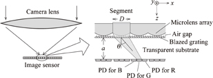
Fig. 1. A concept image of the proposal structure.
Download figure:
Standard image High-resolution imageThe size of PD generally used in compact digital camera ranges from 8 to 1.5 µm. Each segment includes at least three PDs for RGB color splitting and is three times larger than the PD size. We consider and discuss cases of segment size D of 5 and 10 µm in this paper.
The saw-tooth height h giving the highest efficiency for a designed wavelength λD is given by

where ng and na denote refractive indices of the grating material and the air, respectively. Smaller h is better from the viewpoints of diffraction efficiency and fabrication convenience. We chose TiO2 as the grating material to give a large index difference ng − na of 1.60. Then h was calculated to be 0.34 µm for λD = 0.54 µm. The dependence of the diffraction efficiency of the blazed grating on wavelength λ can be approximately expressed by

Calculated wavelength dependence of the 1st-order diffraction efficiency is depicted in Fig. 2. The efficiency was predicted to be higher than 0.8 for a wavelength range from 0.43 to 0.72 µm, indicating no serious degradation within the detection wavelength range.
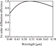
Fig. 2. Calculated wavelength dependence of the 1st-order diffraction efficiency.
Download figure:
Standard image High-resolution imageLarger deflection angle gives better color separation but causes excess broadening of the focal spot on the PD plane. The deflection angle θ is given by

where ns and Λ represent the refractive index of the substrate and the grating period of the blazed grating, respectively. We chose Λ = 1.22 µm. Deflection angles are calculated to be 15.0, 17.6, and 20.4° for wavelength λ of 0.46 µm (B), 0.54 µm (G), and 0.62 µm (R), respectively. Deflected beams should be collected and detected within the segment size of D. Substrate thickness a should be short enough to avoid undesirable broadening of the focal spot due to diffraction. On the other hand, smaller focal spot size and PD size may cause an increase of an optical loss due to the relatively larger gaps between neighboring PDs. We decided the sum of three PD lengths to be 0.8 times D. Thickness a was determined to be 27.5 µm for D = 10 and 14 µm for D = 5 µm from the FDTD simulation results as shown in the next section. Structural parameters are summarized in Table I.
Table I. Designed structural parameters for D =10 and 5 µm.
| Parameter | D = 10 µm | D = 5 µm |
|---|---|---|
| Focal length of the microlens f (µm) | 30 | 15 |
| Refractive index of grating material ng | TiO2: 2.60 | |
| Refractive index of substrate ns | SiO2: 1.46 | |
| Substrate thickness a (µm) | 27.5 | 14 |
| Grating height h (µm) | 0.338 | |
| Grating period Λ (µm) | 1.22 | |
3. FDTD simulation results
3.1. Case of D = 10 µm
Color-splitting performance of the device for D = 10 µm was simulated by 2D FDTD method. Calculated examples of electric field distributions of waves propagating in the structure are shown in Fig. 3.
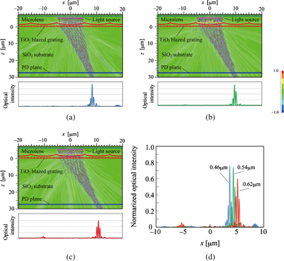
Fig. 3. Examples of electric field distributions calculated by 2D FDTD method with D = 10 µm and wavelengths of 0.46 (a), 0.54 (b), and 0.62 µm (c). Optical intensity distributions on the PD plane (d).
Download figure:
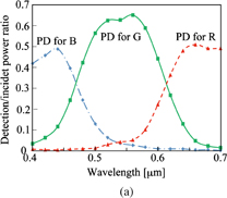
Standard image High-resolution imageA light source was set at Z = −5.0 µm and a wave was launched to Z-direction. The source width was 10 µm in X-direction and had uniform optical intensity. The microlens array was set at Z = −2.0 µm, and the blazed grating was at Z = 0 µm. The amplitude of the electric field is shown by the colors referred in the bar scale on the right of Fig. 3. Most of the power was condensed on a PD plane at Z = 27.5 µm for each wavelength. Antireflection coatings on both sides of blazed gratings were assumed for clear view, namely 0.0837-µm-thick layer of refractive index 1.612 on the boundary of TiO2 and air and 0.0693-µm-thick layer of the refractive index 1.948 on the boundary of TiO2 and SiO2 substrate. Bottom curves in Figs. 3(a)–3(c) show intensity distributions on the PD plane and are joined in Fig. 3(d). RGB lights were split to three positions in a segment of 8 µm length. Curves in Fig. 3 show optical-intensity distributions at a certain instant and then fine structures can be seen. Optical intensities detected by PDs are time averaged ones and are given by envelopes of the fine structures. Spectral sensitivity curves with PD size of 2.6 µm are shown in Fig. 4(a). Detection sensitivities were not balanced among three PDs. Sensitivity curves were improved to be almost ideal NTSC specifications10) when PD sizes were adjusted to 3.0 µm for B, 1.6 µm for G, and 3.4 µm for R as shown in Fig. 4(b). This time, we assumed no gap between PDs.
Download figure:
Standard image High-resolution image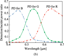
Fig. 4. Calculated spectral sensitivity curves for D = 10 µm and PD sizes of 2.6 µm for all RGB (a), and PD sizes of 3.0 µm for B, 1.6 µm for G, and 3.4 µm for R (b).
Download figure:
Standard image High-resolution imageYou can see no remarkable 0th-order diffraction in Fig. 3(d), but there are several-percentage 2nd-order diffraction for 0.46 µm wavelength and −1st-order diffraction for 0.62 µm wavelength. These undesirable diffractions reduce power utilization efficiency and cause crosstalk noises. With respect to the crosstalk noises, they will be able to be removed electronically by processing signals detected by neighboring segments if necessary since the diffraction efficiencies can be predicted.
A light source of uniform optical intensity within a segment is considered, indicating that some deformation may occur in the sensitivity curves when there is a remarkable intensity distribution in the incident light within the segment.
3.2. Case of D = 5 µm
Spectral sensitivities for D = 5 µm were also calculated. The optical intensity distributions normalized by the incident power on the PD plane are depicted in Fig. 5(a). Spectral sensitivity curves for PD size of 1.3 µm are shown in Fig. 5(b). Obtained sensitivities were not well balanced. The sensitivity curves for PD sizes of 1.5 µm for B, 0.9 µm for G, and 1.6 µm for R are shown in Fig. 5(c). Peak levels of the curves were balanced. However, undesirable color overlaps arise. For example, 10% of G color is detected by PDs assigned to R and B colors. Thus the color splitting feature is not good as the case of D = 10 µm.
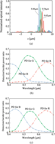
Fig. 5. Electric-field distribution examples calculated for D = 5 µm (a), and spectral sensitivity curves for PD sizes of 1.3 µm for all RGB (b), and PD sizes of 1.5 µm for B, 0.9 µm for G, and 1.6 µm for R (c).
Download figure:
Standard image High-resolution image3.3. Comparison of spectral sensitivity curves
Utilized optical powers and color splitting performances of the device with D = 10 µm are summarized in Table II. For example, 54% of the incident wave power of 0.46 µm wavelength is detected by the PD assigned to B color, while 1 and 10% are detected by the PDs assigned to R and G colors, respectively. The sum of them gives the power utilization efficiency to be 65%. Efficiencies for 0.54 and 0.62 µm wavelength were predicted to be 71 and 64%, respectively. We defined a color separation degree by the ratio of the power detected by the corresponding PD against the total power detected by three PDs. Higher degree indicates better color splitting performance. The degrees are calculated to be from 0.80 to 0.86. The efficiencies and degrees for the device with D = 5 µm are shown in Table III. The efficiencies are similar to but the color separation degrees are almost 0.2 lower than those of the case of D = 10 µm. Values for Bayer mosaic with typical RGB filters are also listed for comparison in Table IV. A half of PD area is assigned to G color while a quarter to each of B and R colors. The incident wave of 0.46 µm wavelength is detected by PDs assigned to R, G, and B colors with filter transparencies of 3, 28, and 88%, respectively. Then the power utilization efficiency is given by 3/4 + 28/2 + 88/4 = 35%. The utilization efficiencies of both of the proposal structures designed with D = 10 and 5 µm were estimated to be almost twice for wavelengths of 0.46 and 0.62 µm and higher for 0.54 µm in comparison to the case of the Bayer color filter. The color separation degrees of the device with D = 10 µm are considerably higher for wavelengths of 0.46 and 0.62 µm and a little bit lower for 0.54 µm in comparison to the Bayer color filter. The degrees of the device with D = 5 µm are higher for 0.46 µm but lower for 0.54 and 0.62 µm in comparison to the Bayer color filter.
Table II. Predicted detection power normalized by the incident power and color separation degree in the proposal structure with D = 10 µm.
| Incident wavelength (µm) | |||
|---|---|---|---|
| 0.46 | 0.54 | 0.62 | |
| Detected by PD for R (%) | 1 | 8 | 55 |
| Detected by PD for G (%) | 10 | 57 | 7 |
| Detected by PD for B (%) | 54 | 6 | 2 |
| Power utilization efficiency (%) | 65 | 71 | 64 |
| Color separation degree | 0.83 = 54/65 | 0.80 = 57/71 | 0.86 = 55/64 |
Table III. Predicted detection power normalized by the incident power and color separation degree in the proposal structure with D = 5 µm.
| Incident wavelength (µm) | |||
|---|---|---|---|
| 0.46 | 0.54 | 0.62 | |
| Detected by PD for R (%) | 3 | 12 | 41 |
| Detected by PD for G (%) | 14 | 44 | 19 |
| Detected by PD for B (%) | 46 | 14 | 3 |
| Power utilization efficiency (%) | 63 | 70 | 63 |
| Color separation degree | 0.73 = 46/63 | 0.63 = 44/70 | 0.65 = 41/63 |
Table IV. Predicted detection power normalized by the incident power and color separation degree in Bayer mosaic with typical RGB filters.
| Incident wavelength (µm) | |||
|---|---|---|---|
| 0.46 | 0.54 | 0.62 | |
| Detected by PD for R (%) | 1 | 4 | 25 |
| Detected by PD for G (%) | 14 | 45 | 8 |
| Detected by PD for B (%) | 22 | 5 | 1 |
| Power utilization efficiency (%) | 35 | 54 | 34 |
| Color separation degree | 0.63 = 22/35 | 0.83 = 45/54 | 0.74 = 25/34 |
4. Preliminary experimental work
4.1. Device fabrication
A fabrication process is shown in Fig. 6. SiO2 of 500 µm thickness was used as a substrate. TiO2 was deposited on it by RF sputtering. The refractive index of the deposited TiO2 film was measured to be 2.52. A blazed grating of resist was formed by an electron-beam (EB) direct writing exposure with dose control. The obtained resist grating was transferred to TiO2 by reactive ion etching.
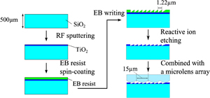
Fig. 6. Fabrication process of a test sample.
Download figure:
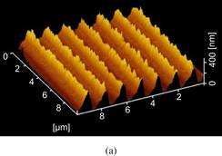
Standard image High-resolution imageSurface profiles of the fabricated TiO2 blazed gratings were measured by an atomic-force microscope. Example of the measured profile is shown in Fig. 7. Grating height was measured to be 350 nm. Obtained blazed shapes differ slightly from the ideal one. The deformation would increase undesirable diffractions and crosstalk noises.
Download figure:
Standard image High-resolution image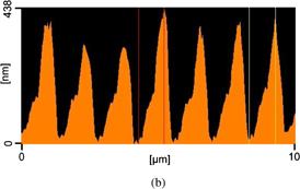
Fig. 7. 3D (a) and cross-sectional (b) views of the fabricated blazed grating measured by atomic force microscope.
Download figure:
Standard image High-resolution imageThe fabricated blazed grating and a honeycomb array of microlenses of 15 µm cell diameter were aligned, contacted face-to-face and fixed. Each microlens has six nearest neighbors. Nearest neighboring microlenses were aligned along y-axis, indicating that pitches were 15 µm along y-axis while 26 µm along x-axis.
4.2. Characterization
An optical setup for characterization is illustrated in Fig. 8. Laser beams of wavelengths of 633 nm (R), 532 nm (G), and 473 nm (B) were combined and introduced to the fabricated device. Diffraction behavior was observed through an objective lens by a CCD camera. The objective lens of numerical aperture of 0.80 was used to collect diffraction waves.
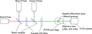
Fig. 8. Optical setup for characterization.
Download figure:
Standard image High-resolution imageObtained diffraction images on the PD plane for wavelengths of 473, 532, and 633 nm are shown in Figs. 9(a), 9(b), and 9(c), respectively. Bottom curves in Figs. 9(a)–9(c) show intensity distributions averaged along y-direction and are joined in Fig. 9(d). Only two segments are shown. The pitch was 26 µm as above-mentioned. It was confirmed that the 1st-order diffraction was dominant in each case. The 0th-order diffraction showed the minimum for wavelength of 532 nm in comparison to other wavelengths of 473 and 633 nm. This result is consistent to theoretical prediction.
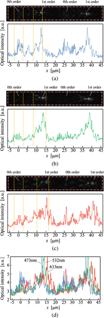
Fig. 9. Optical intensity images and intensity distribution curves on the same plane for wavelength 473 nm (a), 532 nm (b), and 633 nm (c). Three curves are shown in (d) together.
Download figure:
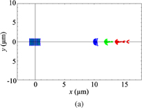
Standard image High-resolution imageWe used a SiO2 substrate of 500 µm thickness different from the designed value for experimental convenience. As a result, the optical intensity distributions on the CCD are different from the ones with substrate thickness of a = 27.5 µm due to refraction on the rear face of the substrate. The refraction effect can be roughly estimated by the ray tracing method. Figure 10 summarizes intensity distributions of an image on a CCD plane with a = 27.5 µm (a) and an imaginary image on the plane observed through the transparent substrate of a = 500 µm (b). By counting the spot broadening effect due to diffraction, we assumed that 1st-order-diffraction light spread over 8 < x < 13 µm for B, 8 < x < 15 µm for G, and 10 < x < 16.5 µm for R. On the other hand, we also assumed that 0th-order-diffraction light spread over −2.5 < x < 2.5 µm for all RGB. Under this assumption, we calculated the optical powers of the 1st- and 0th-order diffractions from Fig. 9 for each wavelength. We did not observe −1st-order diffraction. Then we roughly estimated the diffraction efficiency by the power ratio of the 1st-order diffraction against the sum of the 1st- and 0th-order diffractions to be 61, 80, and 76% for B, G, and R, respectively.
Download figure:
Standard image High-resolution image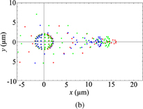
Fig. 10. Ray crossing points on the PD plane calculated by ray tracing method for estimating refraction effect. The 0th- and 1st-order diffractions are shown. (a) Results for 27.5-µm-thick substrate with no refraction effect. (b) Imaginary ray crossing points of the 1st-order diffractions when 500-µm-thick substrate was used.
Download figure:
Standard image High-resolution image
5. Conclusions
We proposed and discussed an optical device for high-efficiency color image sensing. A blazed grating of high-refractive-index material of TiO2 was considered to reduce saw-tooth height. The devices were designed for segment sizes of 5 and 10 µm. Performances were predicted by using 2D FDTD method and discussed for practical applications. The power utilization efficiency was predicted to be considerably higher in comparison to normal case using color filters. We also fabricated a prototype for preliminary demonstration. Color-splitting behavior was successfully observed. Although it was difficult to measure the power utilization efficiency directly, we roughly estimated the efficiency to be 60%. We can conclude that the power utilization efficiency is improved by using the proposed device.
Although incident beam was assumed to be normal against the CCD plane in this paper, incident beam angle depends on the location of a segment in the image sensor as is easily predicted from Fig. 1. The incidence angle is normal at the center segment but gradually varies to the maximum tilt at the edge segments. As a result, diffraction angles vary for a uniform blazed grating. Although the efficiency reduction is not so serious, position shift of PDs will be required to give the optimum sensitivity curves.
Acknowledgments
This work received a part of financial assistance from A-STEP expansion project of research results of Japan Science and Technology Agency. We thank Mr. Junichi Kubo (NALUX Co., Ltd.) for providing microlens array. We also thank Mr. Yoshio Taguchi (ELIONIX Inc.) for fabricating blazed resist gratings.